

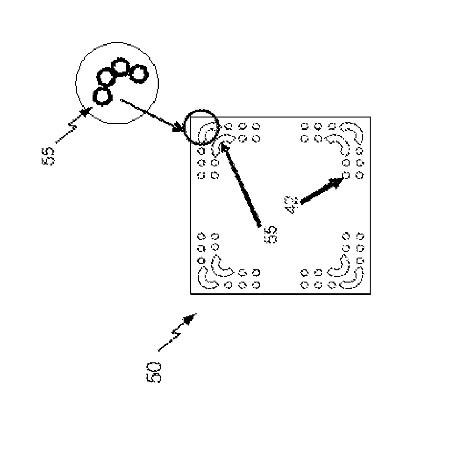
Apparatus and method for controlling semiconductor die warpage
a technology of semiconductor dies and apparatuses, applied in the direction of detecting faulty computer hardware, error detection/correction, instruments, etc., can solve problems such as warpage, substrate warpage or bend, unbalanced stress, etc., and achieve the effect of reducing warpage of semiconductor dies
- Summary
- Abstract
- Description
- Claims
- Application Information
AI Technical Summary
Benefits of technology
Problems solved by technology
Method used
Image

Examples
Embodiment Construction
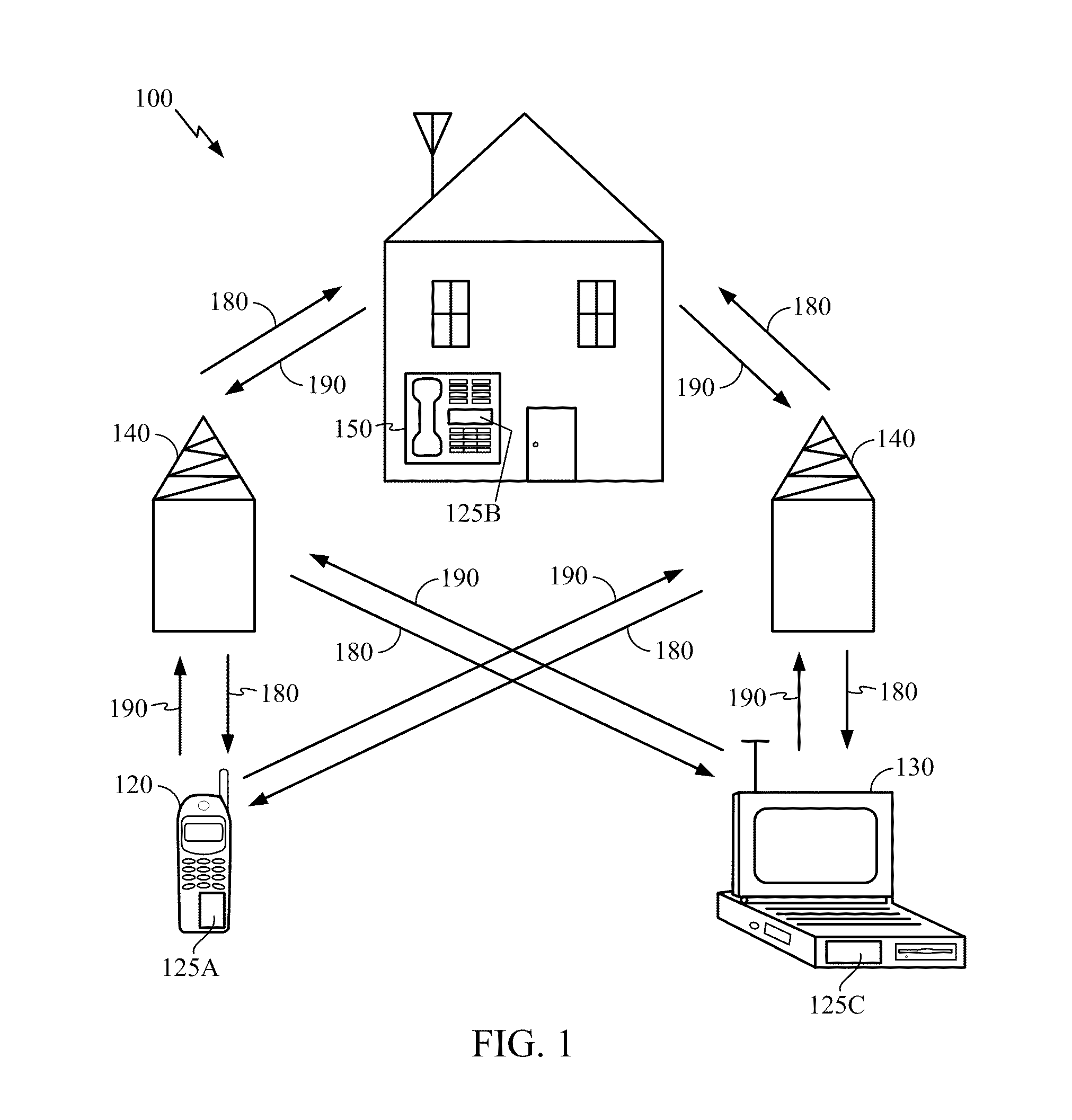
[0020]FIG. 1 is a block diagram showing an exemplary wireless communication system 100 in which an embodiment of the disclosure may be advantageously employed. For purposes of illustration, FIG. 1 shows three remote units 120, 130, and 150 and two base stations 140. It will be recognized that wireless communication systems may have many more remote units and base stations. Remote units 120, 130, and 150 include IC devices 125A, 125B and 125C, that include the disclosed semiconductor die. It will be recognized that any device containing an IC may also include the die disclosed here, including the base stations, switching devices, and network equipment. FIG. 1 shows forward link signals 180 from the base station 140 to the remote units 120, 130, and 150 and reverse link signals 190 from the remote units 120, 130, and 150 to base stations 140.
[0021]In FIG. 1, the remote unit 120 is shown as a mobile telephone, the remote unit 130 is shown as a portable computer, and the remote unit 150...
PUM
 Abstract
Description
Claims
Application Information