Supercharge Your Innovation With Domain-Expert AI Agents!

Textured transparent conductive layer and method of producing it

a transparent, conductive layer technology, applied in the direction of photovoltaic energy generation, energy conversion devices, electrical apparatus, etc., can solve the problems of reduced effectiveness, weak light absorption quantity, and type of method, and achieve satisfactory later growth of the photoelectric layer and good light absorption capacity

Inactive Publication Date: 2014-05-13
UNIV DE NEUCHATEL NEUCHATEL
View PDF12 Cites 0 Cited by
  • Summary
  • Abstract
  • Description
  • Claims
  • Application Information

AI Technical Summary

Benefits of technology

The technical effect of this patent is to provide a TCO layer with a good capacity to trap light and a favorable for subsequent growth of a photoelectric layer. The layer is roughened by plasma etching to promote later growth of the photoelectric layer without significantly reducing its power to diffuse incident light.

Problems solved by technology

However, such a layer leads to a weak quantity of light absorbed, particularly for indirect gap materials, such as microcrystalline silicon and, as a result, a reduced effectiveness.
This type of method does, however, suffer several drawbacks.
First, the cathode sputtering equipment and the necessary targets are relatively expensive, which substantially overloads the price of the cells thus produced.
Secondly, etching of the TCO layer is delicate.
It must therefore be dosed carefully, failing which one obtains, for the TCO layer, a surface morphology, in particular large craters, which is not favorable to optical trapping, as well as interruptions which are not very favorable to good later growth of the photoelectric layer.
Such an approach, applied to the production of a photovoltaic cell, would lead, due to the deposition by evaporation, to a film of very low roughness, clearly insufficient, in any case, to grant it a an acceptable optical trapping capacity for this application.
The action of an argon plasma on the deposited layer would again serve to reduce the roughness of the layer, which would make it practically incapable of providing the optical trapping function of a photovoltaic cell.
Such micro-asperities do not, however, lend themselves particularly well to good later growth of the photoelectric layer.
Moreover, due to their small size, they do not increase light trapping very much in the range of interest (red and infra-red).
Moreover, the fact that the hollows are flat has the drawback of increasing reflection of the light and, because of this, decreasing the light injected into the photovoltaic device, thereby reducing the photo-generated current accordingly.

Method used


Image

  • Textured transparent conductive layer and method of producing it
  • Textured transparent conductive layer and method of producing it
  • Textured transparent conductive layer and method of producing it

Examples


Embodiment Construction

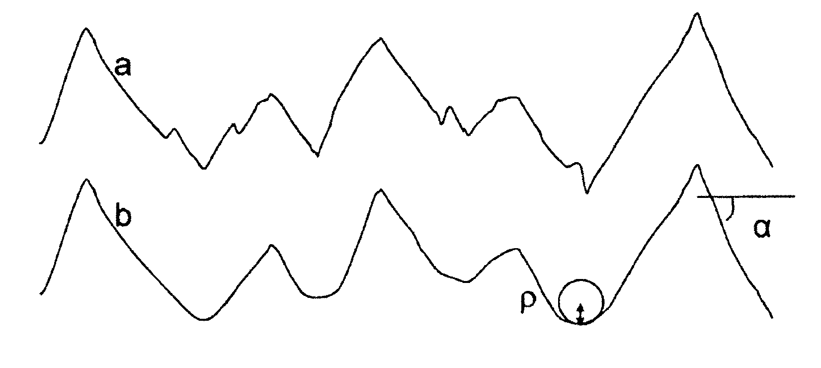
[0027]Before providing a description of the TCO layer according to the invention and its production method, we will recall that a photoelectric device, whether it involves a solar cell or a photodetector, is characterized by its conservation performance η and its optical trapping capacity, the first depending on the second, as long as the collection of photogenerated current is good.

[0028]The conservation performance η of a device of this type is given by the ratio between the electric power supplied by the device and the candle power received, the power supplied being equal to the product:

Short-circuit current(Isc)×Open circuit voltage(Voc)×Fill factor(FF).

[0029]A good indication of the optical trapping capacity is given by the photocurrent density (Iinv) provided by the cell under reverse voltage, this reverse voltage making it possible to extract all photo-generated carrier current and thereby to evaluate the maximum current density of the device, independently of the values of V...


PUM


Abstract

The textured transparent conductive layer according to the invention is deposited on a substrate intended for a photoelectric device and exhibiting a surface morphology formed from a sequence of humps and hollows. It is characterized in that its hollows have a rounded base with a radius of more than 25 nm; the said hollows are virtually smooth, which is to say that, where they exhibit microroughnesses, these microroughnesses have a height on average of less than 5 nm; and its flanks form an angle with the plane of the substrate whose median of the absolute value is between 30° and 75°.

Description

BACKGROUND OF THE INVENTION[0001]1. Field of the Invention[0002]The present invention relates to the field of photoelectric devices. It more particularly concerns a transparent conductive layer deposited on a substrate intended for a photoelectric device in thin layers. A layer of this type is most often called, by specialized, a TCO (transparent conductive oxide) layer or electrode. The invention also concerns a method for producing this electrode.[0003]2. Description of the Related Art[0004]Application of the present invention is particularly interesting for producing photovoltaic cells intended for the production of electrical energy, but it is also applicable, more generally, to any structure in which light radiation is converted into an electrical signal, such as photodetectors.[0005]In the current state of the art, photoelectric devices in thin layers, typically having a thickness smaller than 10 μm, are made up of a substrate that is transparent or not, flexible or stiff, and...

Claims


Application Information

Patent Timeline
Patent Type & Authority Patents(United States)
IPC IPC(8): H01L31/00
CPCY02E10/50H01L31/1884H01L31/0236H01L31/022466H01L31/022483H01L27/142H01L31/18H01L31/0224
Inventor BAILAT, JULIENBALLIF, CHRISTOPHEDOMINE, DIDIER
Owner UNIV DE NEUCHATEL NEUCHATEL
Features
  • R&D
  • Intellectual Property
  • Life Sciences
  • Materials
  • Tech Scout
  • Unparalleled Data Quality
  • Higher Quality Content
  • 60% Fewer Hallucinations
Learn More