

Semiconductor memory device and method of manufacturing the same
a memory device and semiconductor technology, applied in the direction of semiconductor devices, basic electric elements, electrical appliances, etc., can solve the problems of increasing the thickness of the cell region and the peripheral region, and the complexity of the formation of the transistor in the peripheral region, so as to reduce the number of process steps, reduce the thickness difference between the cell region and the peripheral region, and facilitate the formation
- Summary
- Abstract
- Description
- Claims
- Application Information
AI Technical Summary
Benefits of technology
Problems solved by technology
Method used
Image

Examples
Embodiment Construction
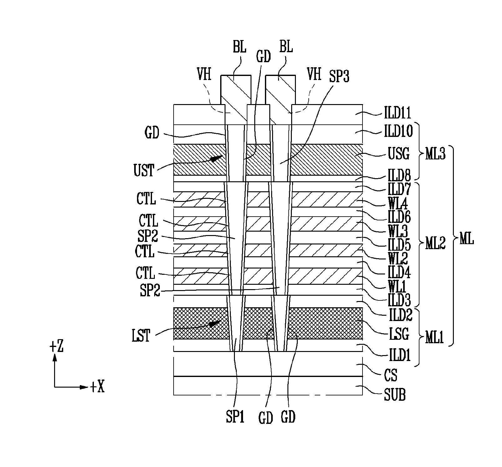
[0047]Hereinafter, some exemplary embodiments of the present disclosure will be described in detail with reference to the accompanying drawings. The figures are provided to allow those having ordinary skill in the art to understand the scope of the embodiments of the disclosure.
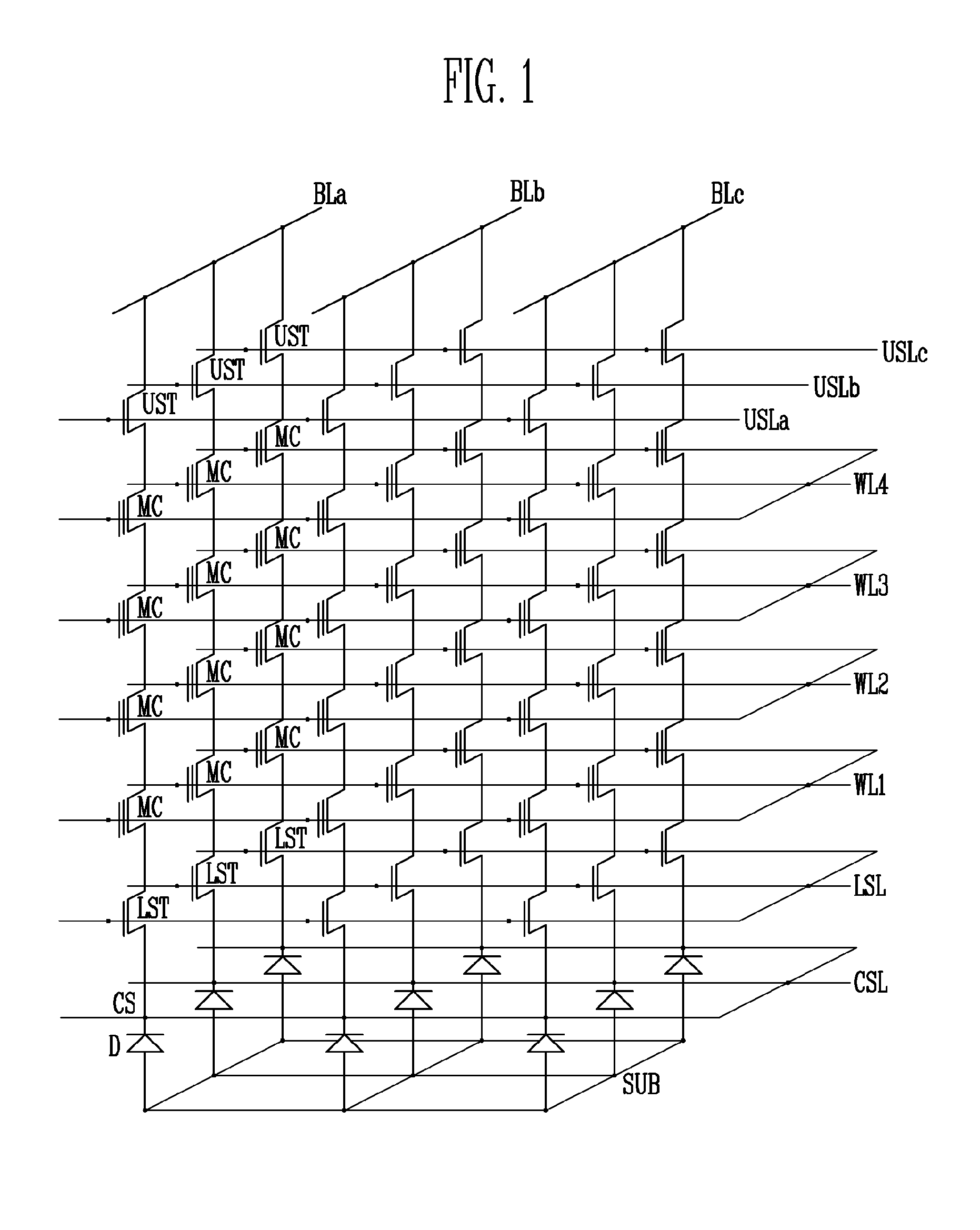
[0048]FIG. 1 is an equivalent circuit diagram of a flash memory array having a bit-cost scalable (BiCS) structure included in a semiconductor memory device according to an embodiment of the present invention.
[0049]Referring to FIG. 1, the memory array having the BiCS structure includes a plurality of memory blocks. Each of the memory blocks includes a plurality of memory strings vertically coupled between a substrate SUB and bit lines BLa, BLb, and BLc. An example where three memory strings are coupled to the respective bit lines is illustrated, for the convenience of description. However, the number of bit lines and the number of memory strings coupled to the bit lines may vary according to a design.
[0050]Ea...
PUM
 Abstract
Description
Claims
Application Information