Semiconductor apparatus, inspection method thereof and electric device

a technology of semiconductor devices and inspection methods, applied in the direction of individual semiconductor device testing, basic electric elements, instruments, etc., can solve the problems of deterioration over time, inability to detect the disconnection of printed conductors, continuity inspection cannot be performed for each individual semicircular through holes, etc., to prevent avulsion or disconnection, the effect of reliable inspection of a bad connection

Active Publication Date: 2014-06-10
SHARP KK
View PDF8 Cites 11 Cited by
  • Summary
  • Abstract
  • Description
  • Claims
  • Application Information

AI Technical Summary

Benefits of technology

[0034]However, as described above, the front surface electrode and the back surface electrode of the insulated substrate are connected with each other through the two through hole penetrating electrodes, which are formed in the insulated substrate, in the improved chip-type LED 200. Thus, even if a bad connection occurred between one of the through hole penetrating electrodes and the front surface electrode or back surface electrode of the insulated substrate, the front surface electrode and the back surface electrode of the insulated substrate would be electrically connected with each other through the other one of the through hole penetrating electrodes. This makes it impossible to detect a bad connection occurring in one of the through hole penetrating electrodes, which causes a problem of not being able to provide LED devices of high reliability, in which the front surface electrodes and the back surface electrodes of the insulated substrate are favorably connected with one another through the two through hole penetrating electrodes formed in the insulated substrate, and which experience minimal deterioration over time.
[0035]The present invention is intended to solve the conventional problems described above. The electrode structure of an insulated substrate constituting a front surface implementing type device, in which a semiconductor chip is implemented on the insulated substrate, is formed to have an electrode structure of high reliability, in which the front surface electrode and the back surface electrode thereof are connected with each another through a plurality of connection electrodes. Further, in such an electrode structure, inspection for a bad connection can be reliably performed between the front surface electrode or back surface electrode and any of the plurality of connection electrodes. As a result, it is an objective of the present invention to provide a semiconductor apparatus and an inspect ion method thereof, capable of providing LED devices or IC parts of high reliability and with minimal deterioration over time, as well as an electric device using such a semiconductor apparatus.
[0051]In the present invention, a semiconductor apparatus with a semiconductor element implemented on an insulated substrate, comprises: a substrate front surface electrode formed on a front surface side of the insulated substrate; a substrate back surface electrode formed on aback surface side of the insulated substrate; and a plurality of connection electrodes formed to extend in a thickness direction of the insulated substrate, for electrically connecting the substrate front surface electrode with the substrate back surface electrode, so that the electrode structure of the insulated substrate can be a highly reliable one in which the substrate front surface electrode and the substrate back surface electrode are connected with each other through the plurality of connection electrodes.
[0052]Furthermore, the substrate front surface electrode or the substrate back surface electrode is formed to have a plane pattern separated for each of the plurality of connection electrodes. Accordingly, the application of test voltage in between portions having a separated plane pattern of the substrate front surface electrode or substrate back surface electrode makes it possible to reliably inspect a bad connection between the substrate front surface electrode or substrate back surface electrode and any of the plurality of connection electrodes.
[0053]Furthermore, in the present invention, side surface electrodes, which are the connection electrodes described above, are formed in cutout parts formed in the side surface of the insulated substrate in the substrate thickness direction. Furthermore, the cutout part is covered with an insulation film to prevent the encapsulating resin from entering the cutout part in which the side surface electrode is formed. As a result, avulsion or disconnection can be prevented between the side surface electrode and the back surface electrode due to the entering of the resin into the cutout part.
[0055]According to the present invention as described above, the electrode structure of the insulated substrate, which constitutes the front surface implementing type device, in which a semiconductor chip is implemented on the insulated substrate, is formed to have an electrode structure of high reliability, in which the front surface electrode and the back surface electrode thereof are connected with each other through a plurality of connection electrodes. Further, in such an electrode structure, inspection for a bad connection can be reliably performed between the front surface electrode or back surface electrode and any of the plurality of connection electrodes. As a result, the present invention has an effect of providing an LED device or an IC part with minimal deterioration over time and high reliability.

Problems solved by technology

Thus, there is such a problem as follows: even if there is a bad connection occurring between the side surface electrode within one of the cutout parts and the front surface electrode or back surface electrode of the insulated substrate, and if the front surface electrode and the back surface electrode of the insulated substrate are electrically connected with each other through the side surface electrode of the other cutout part, it is not possible to detect the bad connection occurring in one of the side surface electrodes, resulting in deterioration over time and breakdown in the end.
In such LEDs, deterioration over time has been occurring, which is thought to be due to the disconnection of the printed conductor layers formed within the through holes of the ceramic substrate.
Thus, it is not possible to detect disconnection of the printed conductor within the through hole by visual inspection.
Thus, all of the wiring patterns are electrically connected with one another, and continuity inspection cannot be performed for each of individual semicircular through holes after the electrodes of the LED substrate are formed.

Method used


Image

  • Semiconductor apparatus, inspection method thereof and electric device
  • Semiconductor apparatus, inspection method thereof and electric device
  • Semiconductor apparatus, inspection method thereof and electric device

Examples


embodiment 1

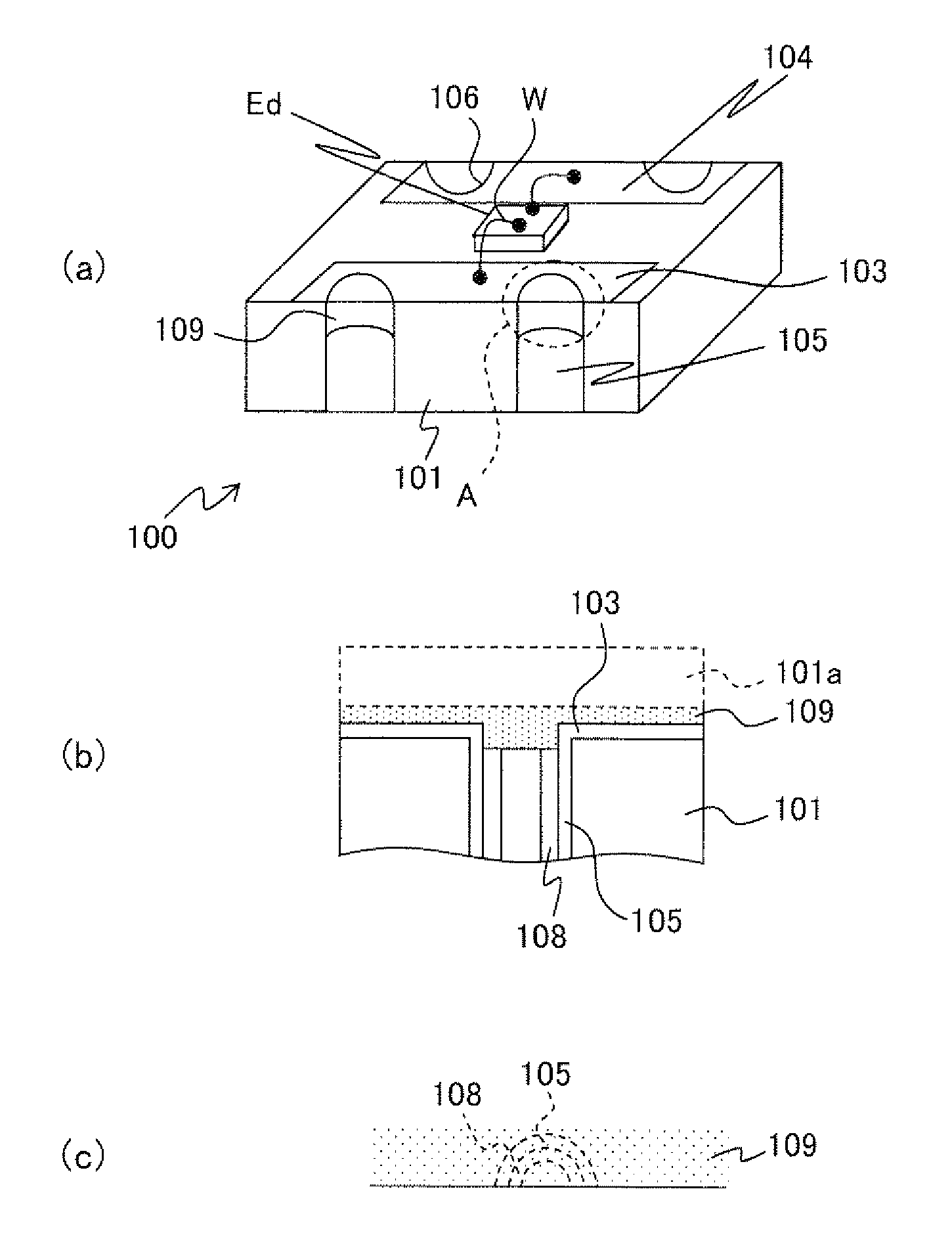
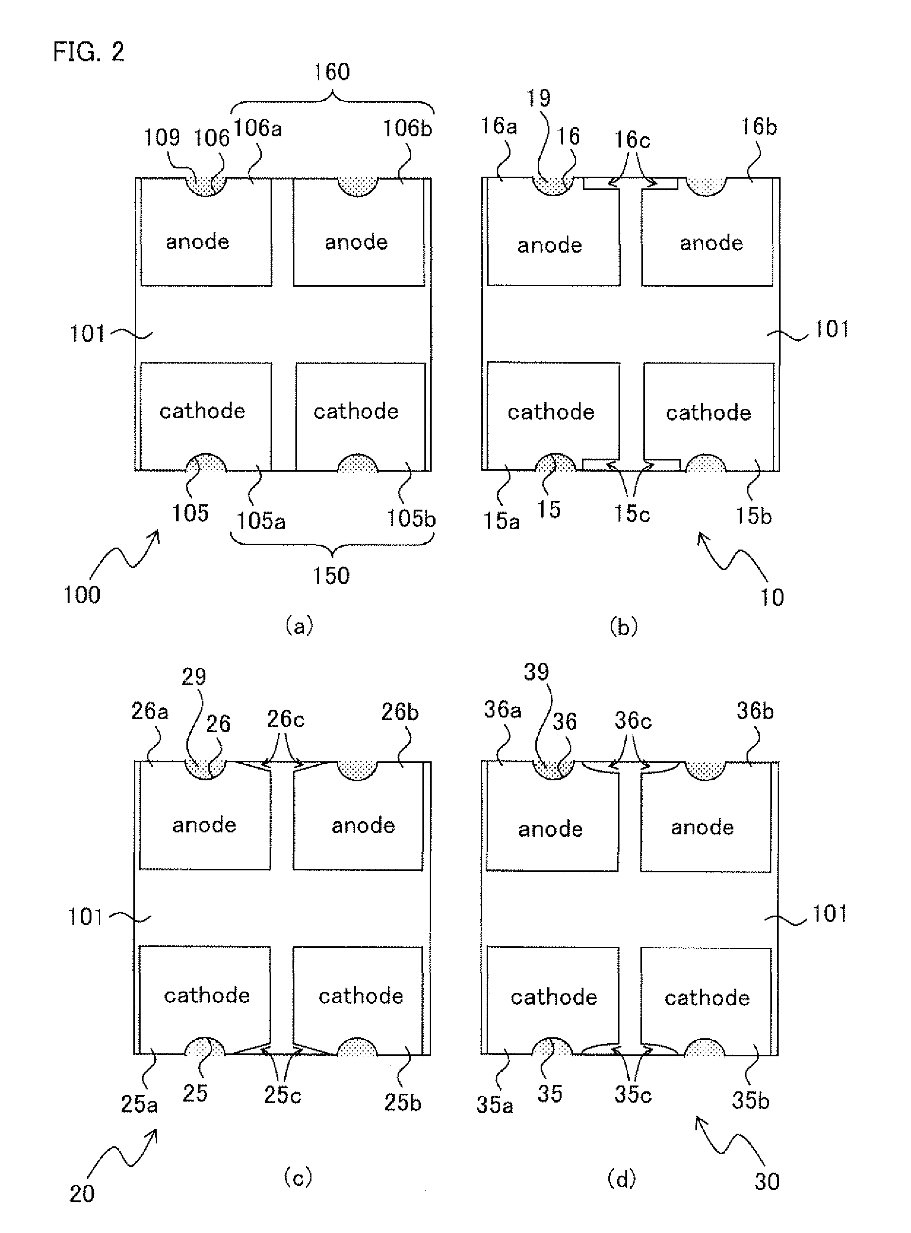
[0096]FIGS. 1 and 2 are each diagrams describing a semiconductor apparatus according to Embodiment 1 of the present invention. FIG. 1(a) is a perspective view illustrating an overall structure thereof. FIG. 1(b) is a partial cross sectional view illustrating a part A in FIG. 1(a). FIG. 1(c) is a plan view corresponding to FIG. 1(b). In addition, FIG. 2(a) illustrates a plane pattern of a back surface electrode of the semiconductor apparatus according to Embodiment 1.

[0097]A semiconductor apparatus 100 according to Embodiment 1 is a semiconductor light emitting apparatus in which a light emitting element Ed is implemented as a semiconductor element on an insulated substrate 101 such as a ceramic substrate.

[0098]The semiconductor apparatus 100 is obtained by implementing the light emitting element (light emitting diode) Ed on the insulated substrate 101, such as a ceramic substrate, in the shape of a rectangle in a plan view, and encapsulating the light emitting element (light emittin...

embodiment 2

[0123]FIGS. 2(b) to 2(d) are each a diagram describing a semiconductor light emitting apparatus according to Embodiment 2, and a variation example thereof, of the present invention. FIG. 2(b) is a diagram describing a semiconductor light emitting apparatus according to Embodiment 2.

[0124]A semiconductor light emitting apparatus 10 according to Embodiment 2 is a modification of the plan view shape of the two back surface individual cathode electrodes constituting the back surface cathode electrode, and the plan view shape of the two back surface individual anode electrodes constituting the back surface anode electrode, in the semiconductor light emitting apparatus 100 according to Embodiment 1 as described above.

[0125]For example, in the semiconductor light emitting apparatus 10 according to Embodiment 2 illustrated in FIG. 2(b), a cutout part 15c of a transversely-long belt-shape may be formed at a portion along a side edge of a insulated substrate 101, where two back surface indivi...

example 1 of embodiment 2

Variation Example 1 of Embodiment 2

[0128]FIG. 2(c) is a diagram describing a semiconductor light emitting apparatus 20 according to Variation Example 1 of Embodiment 2.

[0129]In the semiconductor light emitting apparatus 20 according to Variation Example 1 of Embodiment 2 as illustrated in FIG. 2(c), the shape of the cutout part is a triangular wedge-shape.

[0130]Specifically, as illustrated in FIG. 2(c), a cutout part 25c of a triangular wedge-shape may be formed at a portion along a side edge of an insulated substrate 101, where two back surface individual cathode electrodes 25a and 25b constituting a back surface cathode electrode are opposed with each other. Further, a cutout part 26c of a triangular wedge-shape may be formed at a portion along a side edge of the insulated substrate 101, where two back surface individual anode electrodes 26a and 26b constituting aback surface anode electrode are opposed with each other. The size of the cutout parts 25c and 26c of a triangular wedg...


PUM


Abstract

A semiconductor apparatus according to the present invention with a semiconductor element implemented on an insulated substrate comprises: a substrate front surface electrode formed on a front surface side of the insulated substrate and connected with an element electrode of the semiconductor element; a substrate back surface electrode formed on a back surface side of the insulated substrate and electrically connected with the substrate front surface electrode; and a plurality of connection electrodes, extending in a thickness direction of the insulated substrate from one side to the other side of a front surface and a back surface thereof, for electrically connecting the substrate front surface electrode with the substrate back surface electrode, where the substrate front surface electrode or the substrate back surface electrode is formed to have a plane pattern separated for each of the plurality of connection electrodes.

Description

[0001]This nonprovisional application claims priority under 35 U.S.C. §119(a) to Patent Application No. 2010-192898 filed in Japan on Aug. 30, 2010, the entire contents of which are hereby incorporated by reference.BACKGROUND OF THE INVENTION[0002]1. Field of the Invention[0003]The present invention relates to a semiconductor apparatus and an inspection method thereof as well as an electric device. For example, the present invention relates to a semiconductor apparatus of a surface mounting type, in which a semiconductor chip, such as an LED (Light Emitting Diode) chip, is implemented on an insulated substrate; a method for inspecting such a semiconductor apparatus; and an electric device using such a semiconductor apparatus.[0004]2. Description of the Related Art[0005]Conventionally, semiconductor light emitting diodes include a chip-type LED and a cannonball-type lamp shape LED. Such a chip-type LED, which can be a thin type, is used as a light source of various display panels, ba...

Claims


Application Information

Patent Timeline
Patent Type & Authority Patents(United States)
IPC IPC(8): H01L33/52
CPCH01L2924/014H01L2224/32225H01L2924/01005H01L2224/48465H01L23/49827H01L2924/12041H01L2224/48227H01L33/62H01L2224/48091H01L2924/01006H01L2924/01078H01L2224/73265H01L2924/01033H01L24/32H01L2924/01047H01L2224/97H01L24/48H01L2924/15787H01L2924/01074H01L24/97H01L2924/181H01L24/73H01L2924/00014H01L2224/83H01L2224/85H01L2924/00012H01L2924/00H01L2224/45099H01L2224/45015H01L2924/207
Inventor OHTA, MASAYUKITATSUMI, MASAKISOTA, YOSHIKITAMAKI, KAZUOYAMAGUCHI, SHINJIHARADA, MASAMICHIITO, SHINKIMURA, TOMOSHIINADA, YOSHIFUMI
Owner SHARP KK
Why Eureka
Try Eureka