RFID antenna circuit

a technology of antenna circuit and antenna, applied in the direction of burglar alarm mechanical actuation, burglar alarm by hand-portable object removal, instruments, etc., can solve the problems of reducing the efficiency of the antenna, reducing the communication distance or reducing the transmission of energy or information, and reducing the transmission efficiency. , the effect of improving the transmission conditions

Active Publication Date: 2014-06-10
ERAY INNOVATION
View PDF53 Cites 12 Cited by
  • Summary
  • Abstract
  • Description
  • Claims
  • Application Information

AI Technical Summary

Benefits of technology

[0034]The invention generally sets out to obtain an antenna circuit having transmission efficiency and improved transmitting conditions.

Problems solved by technology

As a general rule, the problems with RFID antenna circuits relate to the efficiency of the magnetic antenna of the transponder and reader i.e. to the efficiency of coupling by mutual inductance between the two magnetic antennas, to the transmission of energy and information between the electronic part and its antenna, and to the transmission of energy and information between the two antennas of the RFID system.
In addition to a reduced (2) or largely reduced (2) surface area, very often there are very strong mechanical or electric constraints such as the presence of a battery, a screen or display, a conductor support in the field very close to the antenna.
These various electric and mechanical constraints on the surface lead to reduced efficiency of the antenna, to loss of coupling efficiency, to loss of signal power emitted or received by the antenna, and to reduced communication distance or reduced transmission of energy or information.
However, a quality factor having such a high value is not suitable for RFID / NFC antenna circuits, readers or transponders (cards, tags, USB keys).
For conventional applications or without these constraints, this quality coefficient of the antenna would be too high and would generate a much reduced antenna bandwidth at −3 dB, hence very severe filtering of the modulated emitted or received HF signal through charge modulation (subcarrier of 13.56 MHz at ±847 kHz, ±424 kHz, ±212 kHz, etc.) and too high emitted or received power.
Also the coupling with said antenna, again for conventional applications or without these constraints, would be such that at a short distance between the 2 antennas (<2 cm for example) the mutual inductance created would be such that it would fully mistune the frequency tuning of the two antennas, would cause the power radiated by the reader to collapse, could saturate the radio stages of the silicon chip and even lead to possible destruction of the transponder silicon, this silicon not having infinite calorific dispersion capacity.
One of the disadvantages of the antenna device according to document US-A1-2008 / 0150693 is that it cannot be integrated into an embossed card.
Another disadvantage is that the coupling of this device in read mode with another antenna does not meet the ideal conditions to obtain optimum coupling with a transponder.
This device according to EP-1,031,939 and FR-2,777,141 has the disadvantage of coupling that is much too strong, without guaranteeing the efficiency of increased read distance.
To increase the transmission of emitted or received energy by the antenna, it is possible to add an amplifier in the radio transmission or receiving chain, but this adds to the financial cost and available energy and entails probable distortion on the modulated HF signal.
It is also possible to increase the level of the signal emitted by the silicon, but this is often limited by integration, technological choices, and size.
It is also possible to reduce the internal consumption of the silicon, but current needs for signal cryptography safety, ever increasing memory capacity, and speed of task execution mean that the trend is more in the direction of increased energy consumption.
With very close distances between the 2 antennas (<2 cm) this is not an ideal solution either, since the mutual inductance would be very high, and would lead to ill-functioning of the RFID systems by introducing a very high quality coefficient Q and hence a very low bandwidth.
Finally, it is possible to act on the size of the antenna, but this is a variable which is rarely debatable and is often a constraint.

Method used


Image

  • RFID antenna circuit
  • RFID antenna circuit
  • RFID antenna circuit

Examples


Embodiment Construction

[0150]In what follows, the antenna circuit can either be a circuit emitting electromagnetic radiation via the antenna, or a circuit which receives electromagnetic radiation via the antenna.

[0151]In a first application, the RFID antenna circuit is of transponder type, to function as a portable card, tag, to be integrated in a paper document such as a document issued by an official authority e.g. a passport, USB keys, SIM cards and (U)SIM cards called “RFID or NFC SIM card”, stickers for Dual cards or Dual Interface cards (the sticker itself having an REID antenna), watches.

[0152]In a second application, the REID antenna circuit is of reader type to read i.e. at least receive the signal radiated by the REID antenna of a transponder such as defined in the first case, such as mobile phones, PDAs, computers.

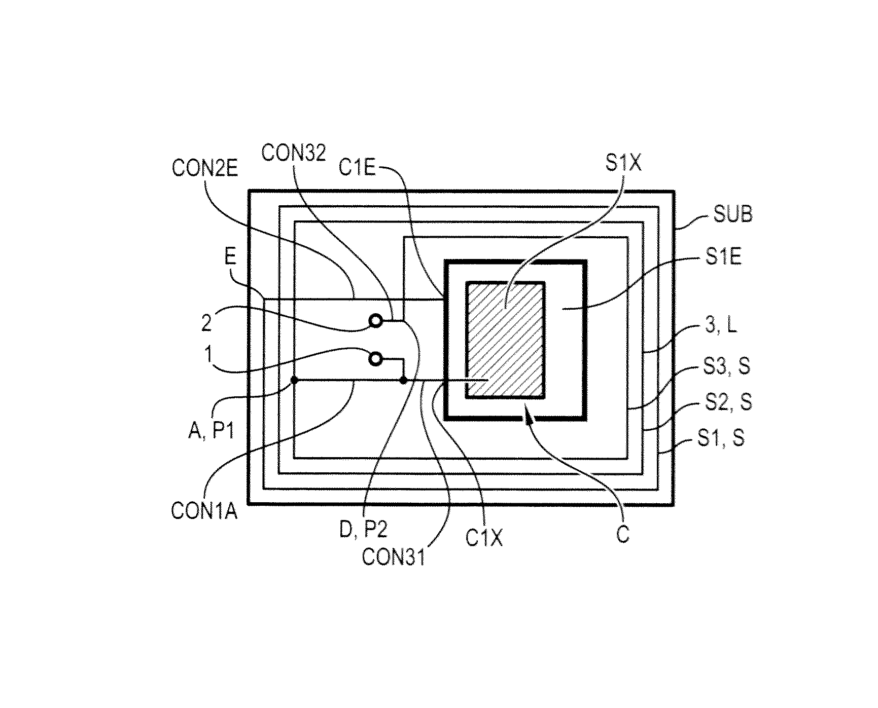
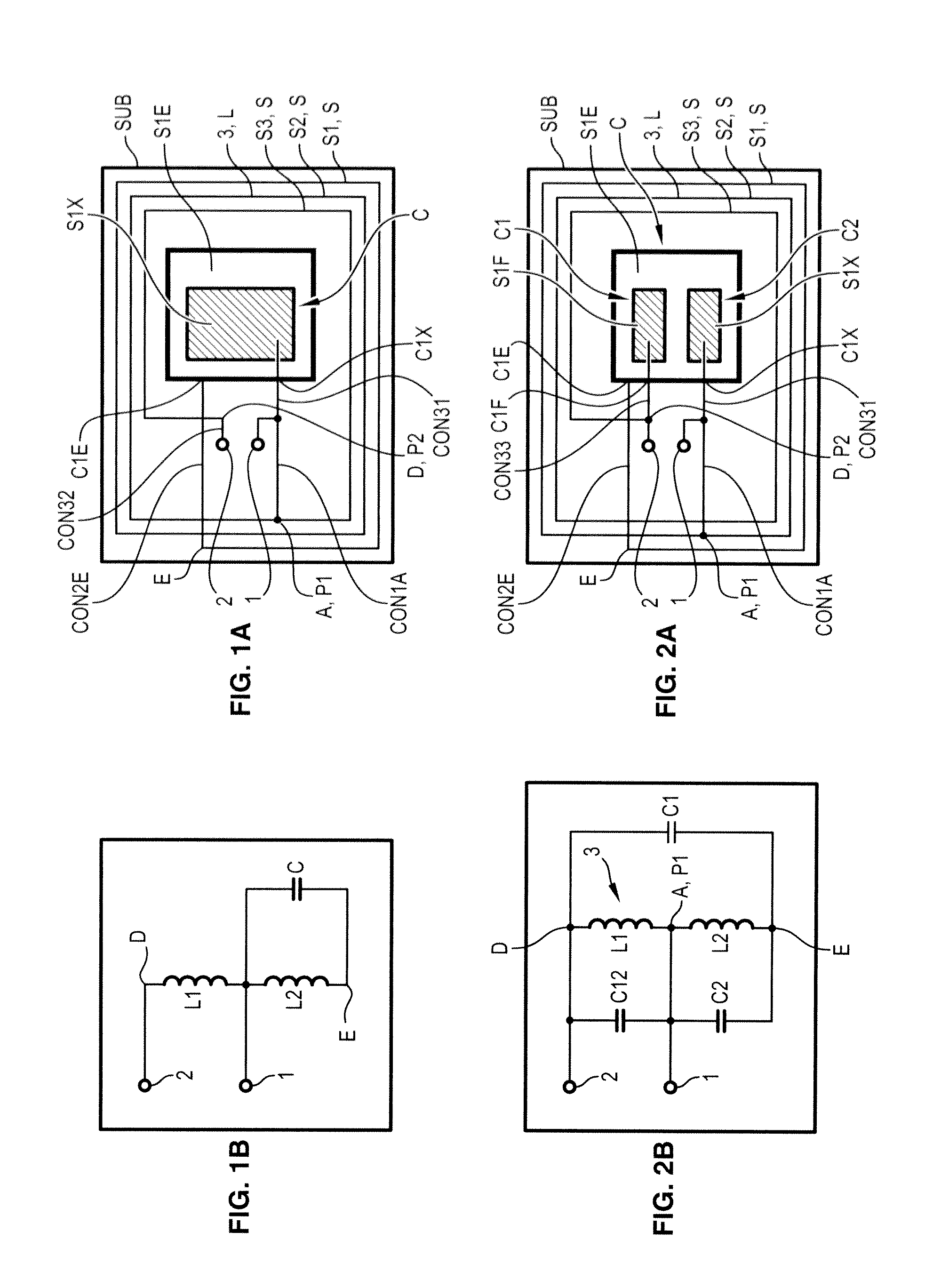
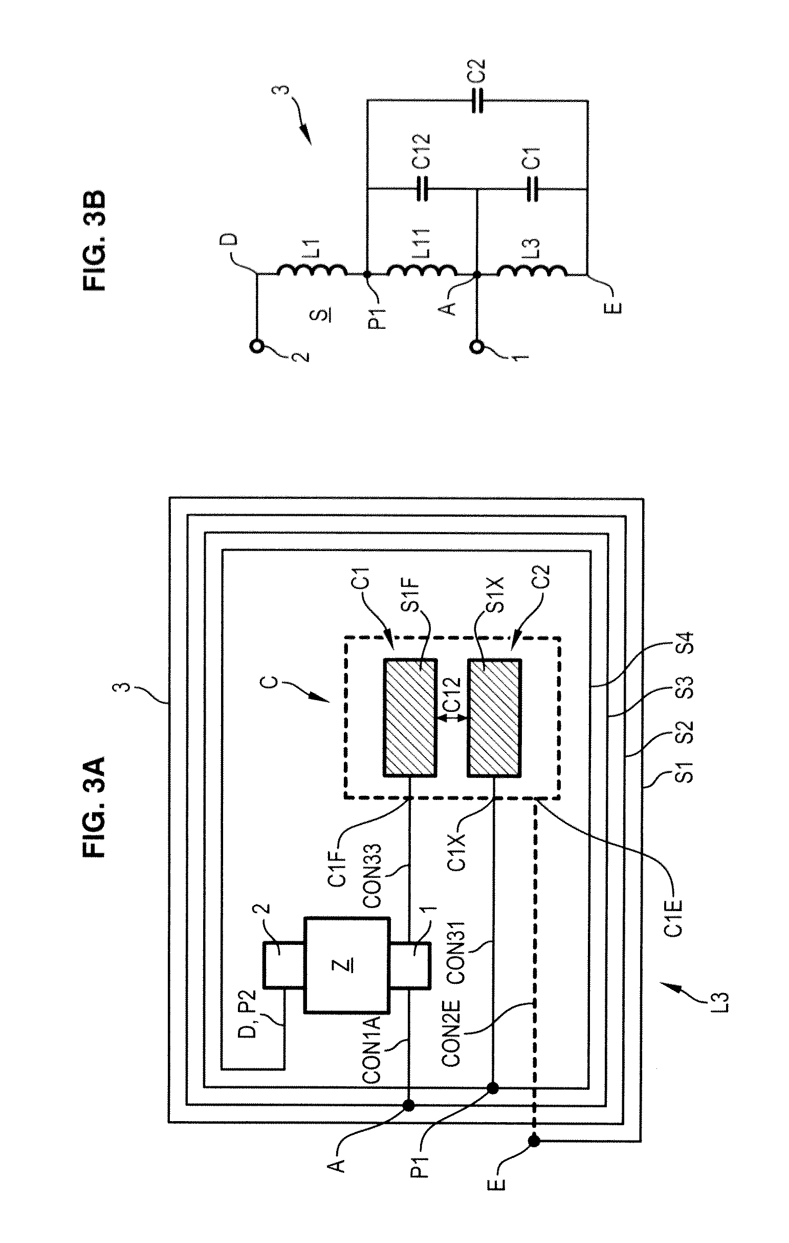
[0153]Generally, the circuit comprises an antenna 3 formed of at least three turns S of a conductor on an insulator substrate SUB. The turns S have an arrangement defining an inductan...


PUM


Abstract

The invention concerns an RFID/NFC antenna circuit. An antenna (L) is formed by at least three turns (S), the antenna having a first end terminal (D) and a second end terminal (E), two access terminals (1, 2) to connect a charge, a tuning capacitance (C1, ZZ) for tuning at a prescribed tuning frequency, an intermediate tap (A) connected to the antenna (L) and distinct from terminals (D, E), a first connector (CON1A) connecting the intermediate tap (A) to terminal (1), a second connector (CON2E) connecting end terminal (E) to the capacitance terminal (C1E). A third connector (CON31, CON32) connects the capacitance terminal (C1X) and the second access terminal (2) respectively to a first point (P1) of the antenna (L) and to a second point (P2) of the antenna (L) connected to the first point of the antenna (L) at least one turn (S) of the antenna (L).

Description

[0001]This is a non-provisional application claiming the benefit of International Application Number PCT / EP2009 / 066749 filed Dec. 9, 2009.BACKGROUND OF THE INVENTION[0002]1. Field of the Invention[0003]The invention concerns an RFID and NEC antenna circuit.[0004]RFID is the abbreviation for Radio Frequency Identification.[0005]NFC is the abbreviation for Near Field Communication.[0006]This is a technique which allows identification of objects using a memory chip or an electronic device which, by means of a radio antenna, is capable of transmitting information to a specialized reader.[0007]2. Description of Related Art[0008]RFID / NFC technology is used in numerous areas, for example in mobile telephones, personal digital assistants PDAs, computers, contactless card readers, the cards themselves which are to be read without contact, but also passports, identification or description tags, USB keys, SIM and (U)SIM cards called “RFID or NEC SIM card”, stickers for Dual or Dual Interface c...

Claims


Application Information

Patent Timeline
Patent Type & Authority Patents(United States)
IPC IPC(8): G08B13/14
CPCH01Q7/00H01Q1/2225
Inventor ERAY, YVES
Owner ERAY INNOVATION
Why Eureka
Try Eureka