Semiconductor device and method of manufacturing the same

a semiconductor and semiconductor technology, applied in the field of semiconductor devices, can solve the problems of cost reduction and difficulty in downsizing the semiconductor device, and achieve the effects of low cost, high reliability and low cos

Active Publication Date: 2014-07-01
RENESAS ELECTRONICS CORP
View PDF29 Cites 6 Cited by
  • Summary
  • Abstract
  • Description
  • Claims
  • Application Information

AI Technical Summary

Benefits of technology

[0010]More specifically, when a thickness of the electronic component 30 is 400 μm, at least 400 μm or larger is required for a diameter L1 of the solder ball 40 including the Cu core 42 having the spacer function, and 400 μm or larger is required for the connecting pitch L2 as well. At this time, if the diameter L1 of the solder ball 40 and the connecting pitch L2 have the same value, the adjacent solder balls 40 contact each other, and therefore, a distance larger than 400 μm is required for the connecting pitch L2, and the downsizing of the semiconductor device is significantly prevented.
[0012]Also, a melting point of the solder 44 such as a ternary-alloy solder made of Sn (tin), Ag (silver), and Cu is about 220° C., and therefore, it is required to set a temperature in reflow heating for the connection of the solder ball 40 to about 245° C. However, thermal deformation of the wiring substrate is increased by the reflow heating for a downsized and thinned semiconductor device, and there is a possibility that reliability of the semiconductor device is significantly decreased. The wiring substrate is significantly influenced by heat easier as a thickness of the wiring substrate is thinner, and therefore, it is disadvantageous to use the solder ball 40 for the connection between the stacked substrates for achieving the downsizing of the semiconductor device and manufacturing cost reduction thereof.
[0016]A preferred aim of the present invention is, in a semiconductor device in which wiring substrates are stacked and sealed by a resin, to achieve a downsized and thinned semiconductor device and provide a high-reliable and low-cost semiconductor device.
[0023]Also, thermal deformation of a wiring substrate used in the semiconductor device is suppressed, so that decrease in reliability of the semiconductor device can be prevented.
[0024]Further, a manufacturing cost of the semiconductor device can be reduced, so that a cheap semiconductor device can be provided.

Problems solved by technology

However, in the electronic-component embedded substrate 48 described in Patent Document 1 and illustrated in FIG. 11, when the solder ball 40 including the Cu core 42 is used for the electrical connection between the lower-layer side wiring substrate 10 and the upper-layer side wiring substrate 20, a connecting pitch L2 of the solder ball 40 is necessarily large, and therefore, there arise a problem that it is difficult to downsize the semiconductor device.
The wiring substrate is significantly influenced by heat easier as a thickness of the wiring substrate is thinner, and therefore, it is disadvantageous to use the solder ball 40 for the connection between the stacked substrates for achieving the downsizing of the semiconductor device and manufacturing cost reduction thereof.

Method used


Image

  • Semiconductor device and method of manufacturing the same
  • Semiconductor device and method of manufacturing the same
  • Semiconductor device and method of manufacturing the same

Examples


Embodiment Construction

[0037]Hereinafter, embodiments of the present invention will be described in detail with reference to the accompanying drawings. Note that components having the same function are denoted by the same reference symbols throughout the drawings for describing the embodiment, and the repetitive description thereof will be omitted.

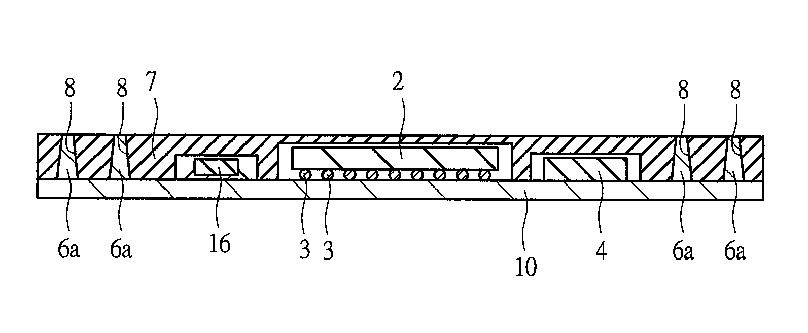
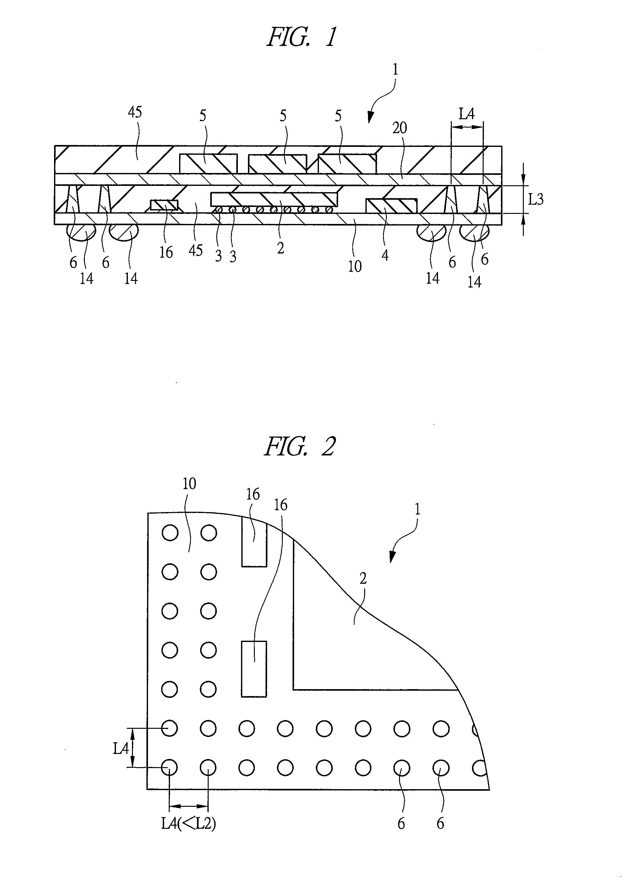
[0038]FIG. 1 is a cross-sectional view of a principal part of a semiconductor device according to the present embodiment, and FIG. 2 is a plan view partially illustrating the semiconductor device illustrated in FIG. 1. Note that, in order to easily understand the structure in FIG. 2, only the lower-layer side wiring substrate 10, the high-frequency power amplifier chip 2, the circuit component 16, and the solder ball 40 arranged on the upper surface of the lower-layer side wiring substrate 10 are illustrated. And, the upper-layer side wiring substrate 20, the sealing resin 45, the antenna switch 4, and wirings on the upper surface of the lower-layer side wiring ...


PUM

PropertyMeasurementUnit
diameteraaaaaaaaaa
diameter L1aaaaaaaaaa
thicknessaaaaaaaaaa

Abstract

In a method of manufacturing a semiconductor device, a second wiring substrate is stacked over a first wiring substrate using a conductive paste, where each wiring substrate has mounted thereon an electronic component. The conductive paste is hardened to form a metal column which forms an electrical connection between the first wiring substrate and the second wiring substrate. The wiring substrates are sealed with a resin. The semiconductor device can be downsized, thinned, and made highly reliable, and its manufacturing cost can be reduced. By using conductive paste for the electrical connection between the wiring substrates, a connecting pitch can be smaller than that in a connecting method of using a solder ball including Cu core, and a connection at low temperature can be achieved. Also, by coating the conductive paste by a print-coating or dispense-coating method, manufacturing is simplified and the manufacturing cost is reduced.

Description

CROSS-REFERENCE TO RELATED APPLICATION[0001]The present application claims priority from Japanese Patent Application No. 2009-271258 filed on Nov. 30, 2009, the content of which is hereby incorporated by reference into this application.TECHNICAL FIELD OF THE INVENTION[0002]The present invention relates to a semiconductor device and a method of manufacturing the same. More particularly, the present invention relates to a technique effectively applied to a semiconductor device and a method of manufacturing the same having a three-dimensional mounting structure in which a plurality of wiring substrates each mounting an electronic component are stacked.BACKGROUND OF THE INVENTION[0003]As high performance of an electronic component has been advanced in recent years, a semiconductor device on which the electronic component is highly integrated has been developed. As such a semiconductor device, for example, an electronic-component embedded substrate which is three-dimensionally mounted is...

Claims


Application Information

Patent Timeline
Patent Type & Authority Patents(United States)
IPC IPC(8): H01K3/22H05K3/30H05K3/36H05K3/00
CPCH01L2924/014H01L2224/32225H01L2924/01005H05K2201/09118H05K3/4614H01L2924/0105H01L21/565H01L2224/48227H01L2224/48091H01L2924/01006H01L2924/15311H01L2224/73265H01L25/16H01L2224/45124H01L2924/01047H01L2924/01013H01L2924/01029H01L23/3128H01L2924/01082H01L24/45H01L23/66H01L2224/8592H01L2924/01004H01L2224/16225H01L2224/48699H05K2203/041H01L2924/01079H01L2224/48472H01L2224/45144H01L2924/19041H05K2203/0733H01L2924/01033H01L2224/48599H01L24/48H05K1/186H01L2924/19105H01L24/73H01L2924/181H01L2924/00014Y10T29/49165Y10T29/49146Y10T29/49124Y10T29/49126H01L2924/00H01L2924/00012H01L2224/85399H01L2224/05599
Inventor KAWANO, KENYAYORITA, CHIKOSHIRAI, YUJI
Owner RENESAS ELECTRONICS CORP
Why Eureka
Try Eureka