APDs using nano-plasmonic metamaterials

a metamaterial and nano-plasmonic technology, applied in the field ofavalanche photodiodes, can solve the problems of low noise, operating temperature substantially affecting both the noise level and bias voltage point of the geiger

Active Publication Date: 2014-07-08
ROCKWELL COLLINS INC
View PDF15 Cites 26 Cited by
  • Summary
  • Abstract
  • Description
  • Claims
  • Application Information

AI Technical Summary

Benefits of technology

[0008]According to one embodiment of the invention there is provided an avalanche photodiode (APD) electro-magnetic radiation (EMR) detector. The APD EMR detector comprises: an EMR absorption region comprising a substantially regular array of nano-particles embedded in a matrix material; a voltage biasing element configured to apply a bias voltage to the matrix material such that electrical current is directly generated in the EMR absor

Problems solved by technology

The carrier multiplication is then mainly due to electrons, resulting in low noise.
With traditional p-n junction APD devices and absorpti

Method used


Image

  • APDs using nano-plasmonic metamaterials
  • APDs using nano-plasmonic metamaterials
  • APDs using nano-plasmonic metamaterials

Examples


embodiments

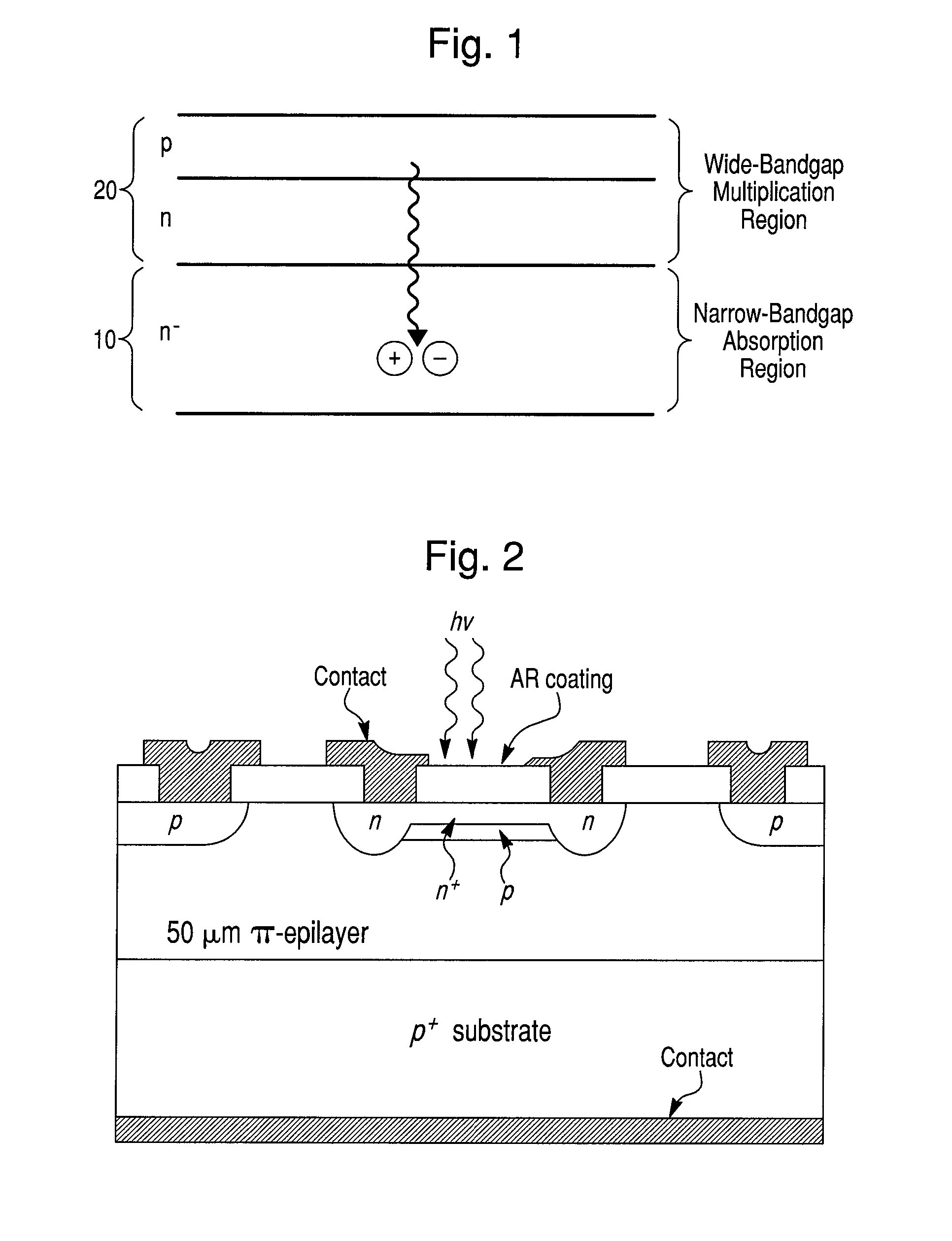
[0058]FIG. 5A illustrates a schematic of an APD EMR detector according to one embodiment. The APD EMR detector includes an EMR absorption region 10, which is the detector material 216, a voltage biasing element 240, and a charge multiplication region 20. The detector material 216 includes a substantially regular array 212 of nanoparticles 210 embedded in a matrix material 214. The voltage biasing element 240 is configured to apply a bias voltage to the matrix material 214 such that electrical current is directly generated based on a cooperative plasmon effect in the detector material when electromagnetic radiation in a predetermined wavelength range is incident upon the detector material, where the dominant mechanism for decay in the cooperative plasmon effect is nonradiative. The charge multiplication region 20 is arranged relative to the EMR absorption region 10 to avalanche multiply the electrical current generated in the EMR absorption region 10.

[0059]The nanoparticles 210 and t...


PUM


Abstract

An avalanche photodiode (APD) electro-magnetic radiation (EMR) detector is described. The detector includes an EMR absorption region, a voltage biasing element, and a charge multiplication region. The EMR absorption region includes a substantially regular array of nano-particles embedded in a matrix material. The voltage biasing element is configured to apply a bias voltage to the matrix material such that electrical current is directly generated in the EMR absorption region based on a cooperative plasmon effect in the detector material when electro-magnetic radiation in a predetermined wavelength range is incident upon the detector material, where the dominant mechanism for decay in the cooperative plasmon effect is non-radiative. The charge multiplication region is arranged relative to the EMR absorption region to avalanche multiply the electrical current generated in the EMR absorption region.

Description

RELATED APPLICATION[0001]This application is a continuation-in-part application of U.S. application Ser. No. 13 / 243,342, filed Sep. 23, 2011, entitled NANO-STRUCTURE ARRAYS FOR EMR IMAGING, the entire contents of which are incorporated by reference.FIELD OF INVENTION[0002]The present disclosure relates to an avalanche photo-diode (APD) including nano-particle materials.BACKGROUND[0003]Avalanche photo-diodes (APDs) have been used as electromagnetic radiation (EMR) detectors, and have applications, such as for single photon counting experiments, imaging and telecommunications.[0004]There are different styles of APDs, including ‘reach-through’ (RAPD), separate absorption-multiplication regions (SAM), separate absorption grading and multiplication (SAGM)—and super-lattice stair-case band-gap designs, which are admixtures of these concepts. For all of these APD designs, incident EMR is absorbed as much as possible in some semiconductor region (absorption region), and the resulting electr...

Claims


Application Information

Patent Timeline
IPC IPC(8): G01T1/02B82Y20/00H01L31/0352H01L31/0232
CPCH01L31/1075B82Y20/00B82Y30/00H01L31/0522H01L31/035218H01L31/02327
Inventor BROWN, ROBERT G.STANLEY, JAMES H.
Owner ROCKWELL COLLINS INC
Why Eureka
Try Eureka