Spurious induced charge cleanup for one time programmable (OTP) memory

a one time programmable and purious charge technology, applied in static storage, digital storage, instruments, etc., can solve the problems of increasing the layout size and cost of memory, weak rotation of the transistors, etc., and achieve the effect of substantially reducing the layout size of the core area and exceeding the operational power requirements

Active Publication Date: 2014-07-15
CHENGDU KILOWAY ELECTRONICS CO LTD
View PDF6 Cites 13 Cited by
  • Summary
  • Abstract
  • Description
  • Claims
  • Application Information

AI Technical Summary

Benefits of technology

[0005]Briefly, in one embodiment of the present invention, a high density, low voltage, and low-power one time programmable (OTP) memory is based on core cells with a one transistor design. A CLEAN pulse is directed to a single shunt device at the output of the column decoder so spurious charges that may have been stored in the floating nodes can be cleaned up. Such arrangement also allows for the simultaneous initialization of bit lines, data lines, and sensing lines to zero. Core area layout size is substantially reduced, and operational power requirements are exceeding low making these particularly suitable in UHF RFID applications.

Problems solved by technology

Spurious charges can be induced from nearby unintended sources causing the transistors to weakly turn on and their sense amplifiers to report a wrong data storage result.
Some of these add special circuits and more devices, substantially increasing the layout size and cost of the memory.

Method used


Image

  • Spurious induced charge cleanup for one time programmable (OTP) memory
  • Spurious induced charge cleanup for one time programmable (OTP) memory
  • Spurious induced charge cleanup for one time programmable (OTP) memory

Examples


Embodiment Construction

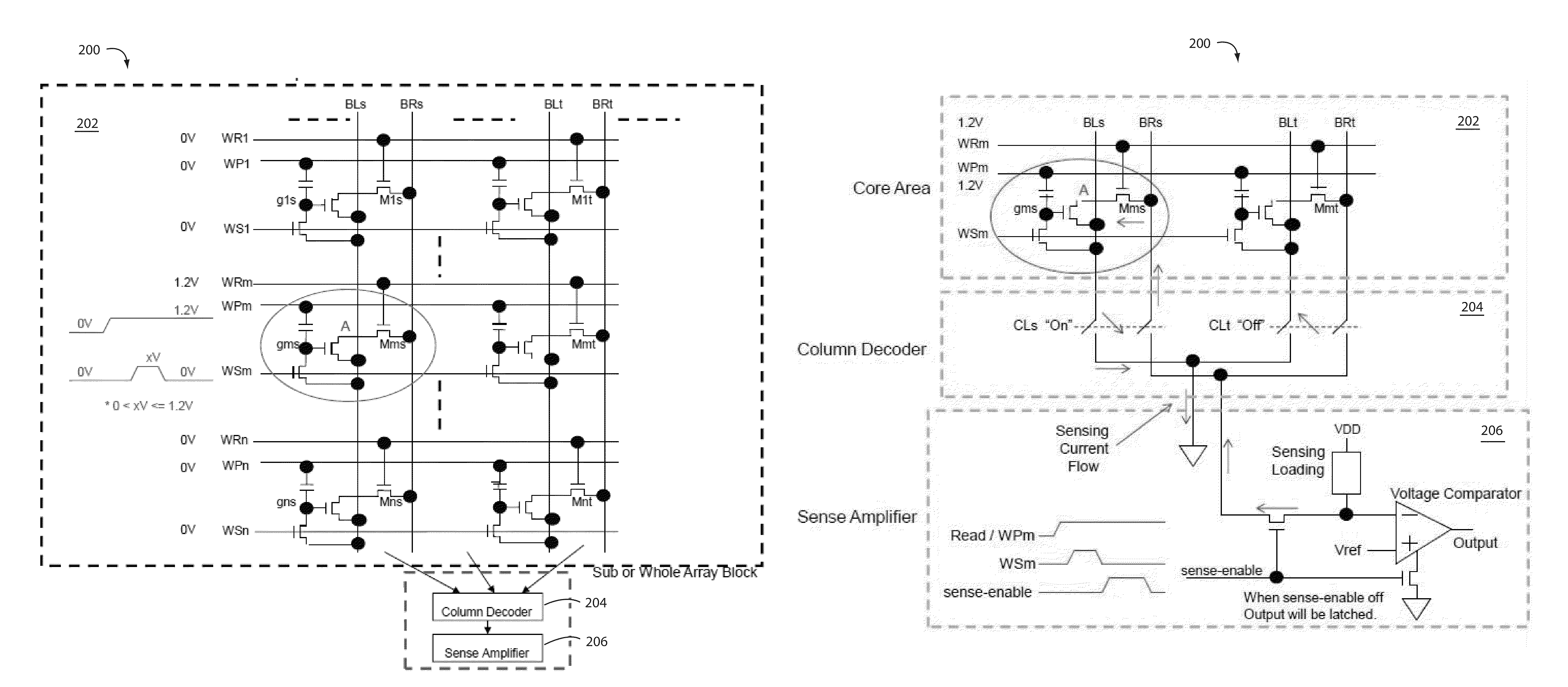
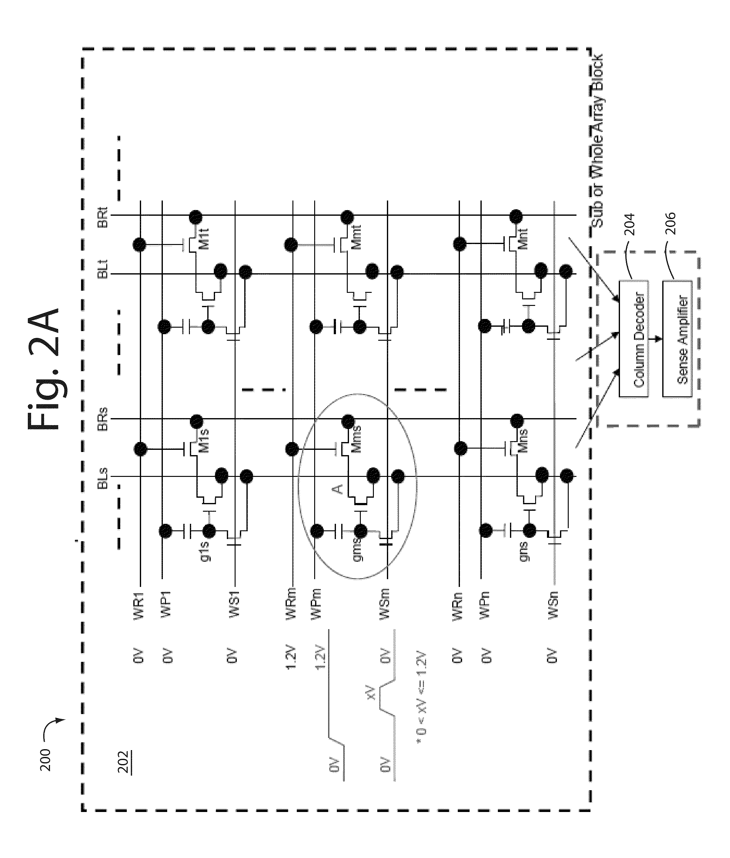
[0012]FIG. 1 and Voltage Table I represent a memory 100 comprising an array block 102 and core cells. Each core cell is based on two transistors (N) and one floating node comprising a capacitor C and gate g.

[0013]

VOLTAGE TABLE ICellV(WP)V(WS)V(BL)V(BR)ProgrammingA SW / SB5.5V2.5V0VfloatingB SW / UB5.5V2.5V2.5VfloatingC UW / SB2.5V0V0VfloatingD UW / UB2.5V0V2.5VfloatingReadA SW / SB1.0V0V0VV sensing +B SW / UB1.0V0VfloatingfloatingC UW / SB0V0V0VV sensing −D UW / UB0V0Vfloatingfloatingsensing line

Where the voltage values can be + / − by 10%˜50% for a 0.13 μm CMOS process, depends on the process and detailed implementation of the decoding circuits. In an 0.18 μm process, these voltages will be correspondingly higher.

[0014]In memory array block 102 the core cells are arranged in rows (m) and columns (s) with internal bit line (BLs) and bit read (BRs) interconnections to corresponding column decoders and sense amplifiers, and write pulse line (WP) and write sense line (WS) row (m) interconnections. Each ...


PUM


Abstract

A high density, low voltage, and low-power one time programmable (OTP) memory is based on core cells with a one transistor design. A CLEAN pulse is directed to a single shunt device at the output of the column decoder so spurious charges that may have been stored in the floating nodes can be cleaned up. Such arrangement also allows for the simultaneous initialization of bit lines, data lines, and sensing lines to zero. Core area layout size is substantially reduced, and operational power requirements are exceeding low making these particularly suitable in HF and UHF RFID applications.

Description

RELATED APPLICATIONS[0001]This Application is a continuation in part (CIP) of U.S. patent application Ser. No. 12 / 796,031, filed Jun. 08, 2010 now U.S. Pat. No. 8,259,518, issued on Sep. 4, 2012, and titled, A NEW LOW VOLTAGE AND LOW POWER XPM CELL, by the present inventors, Jack Zezhong Peng and David Fong. Such Parent Application received a Notice of Allowance that was mailed May 30, 2012.FIELD OF THE INVENTION[0002]The present invention relates to non-volatile memory (NVM) devices and memory cell circuits, and more specifically to high density, low voltage, and low-power one time programmable (OTP) core cells and memories important in HF and UHF RFID applications.BACKGROUND[0003]The core cells in some memory device types are based on NMOS field effect transistors and bit capacitors. The present inventor, Jack Peng, describes the conventional construction of one time programmable (OTP) memory cells in U.S. Pat. No. 6,667,902, issued Dec. 23, 2003. The circuit impedances are extrem...

Claims


Application Information

Patent Timeline
Patent Type & Authority Patents(United States)
IPC IPC(8): G11C7/02
CPCG11C7/02G11C17/16G11C17/18
Inventor PENG, JACK, Z.
Owner CHENGDU KILOWAY ELECTRONICS CO LTD
Why Eureka
Try Eureka