Integrated inertial sensing apparatus using MEMS and quartz configured on crystallographic planes

a crystallographic plane and inertial sensing technology, applied in the direction of turning-sensitive devices, acceleration measurement using interia forces, instruments, etc., can solve the problems of increasing cost, focusing on mems development, and reducing cost, so as to improve device yield in dies, widen the range of applicability, and facilitate use

Active Publication Date: 2014-08-05
MOVELLA INC
View PDF182 Cites 18 Cited by
  • Summary
  • Abstract
  • Description
  • Claims
  • Application Information

AI Technical Summary

Benefits of technology

[0007]According to the present invention, techniques related generally to electronic and mechanical devices are provided. More particularly, the present invention provides an inertial sensing apparatus that is preferably integrated with one or more integrated circuits and / or other micro-electrical mechanical systems, commonly termed MEMS. Merely by way of example, the MEMS devices can include at least an accelerometer, a gyroscope, a magnetic sensor, a pressure sensor, a microphone, a humidity sensor, a temperature sensor, a chemical sensor, a biosensor, an inertial sensor, and others. Additionally, the other applications include at least a sensor application or applications, system applications, and broadband applications, among others. But it will be recognized that the invention has a much broader range of applicability.
[0008]In a specific embodiment, the present invention provides an apparatus for inertial sensing, e.g., an integrated gyroscope and accelerometer device. The apparatus includes a substrate member including a thickness of material. In an embodiment, the apparatus also has a first surface region configured from a first crystallographic plane of the substrate and a second plane region configured from a second crystallographic plane of the substrate. The apparatus has a quartz inertial sensing device coupled to the first surface region, and one or more MEMS inertial sensing devices coupled to the second plane region. Of course, there can be other variations, modifications, and alternatives.
[0009]Many benefits are achieved by way of the present invention over conventional techniques. For example, the present technique provides an easy to use process that relies upon conventional technology. In some embodiments, the method provides higher device yields in dies per wafer with the integrated approach. Additionally, the method provides a process and system that are compatible with conventional process technology without substantial modifications to conventional equipment and processes. Preferably, the invention provides for an improved CMOS integrated circuit device and related methods for a variety of uses. In one or more preferred embodiments, the present invention uses micro-machining techniques, such as those commonly used in the manufacture of MEMS and / or semiconductor devices. Depending upon the embodiment, one or more of these benefits may be achieved. These and other benefits will be described in more throughout the present specification and more particularly below.
[0010]Various additional objects, features and advantages of the present invention can be more fully appreciated with reference to the detailed description and accompanying drawings that follow.

Problems solved by technology

Although highly successful, ICs and in particular MEMS still have limitations.
Similar to IC development, MEMS development, which focuses on increasing performance, reducing size, and decreasing cost, continues to be challenging.
Additionally, applications of MEMS often require increasingly complex microsystems that desire greater computational power.
Unfortunately, such applications generally do not exist.

Method used


Image

  • Integrated inertial sensing apparatus using MEMS and quartz configured on crystallographic planes
  • Integrated inertial sensing apparatus using MEMS and quartz configured on crystallographic planes
  • Integrated inertial sensing apparatus using MEMS and quartz configured on crystallographic planes

Examples


Embodiment Construction

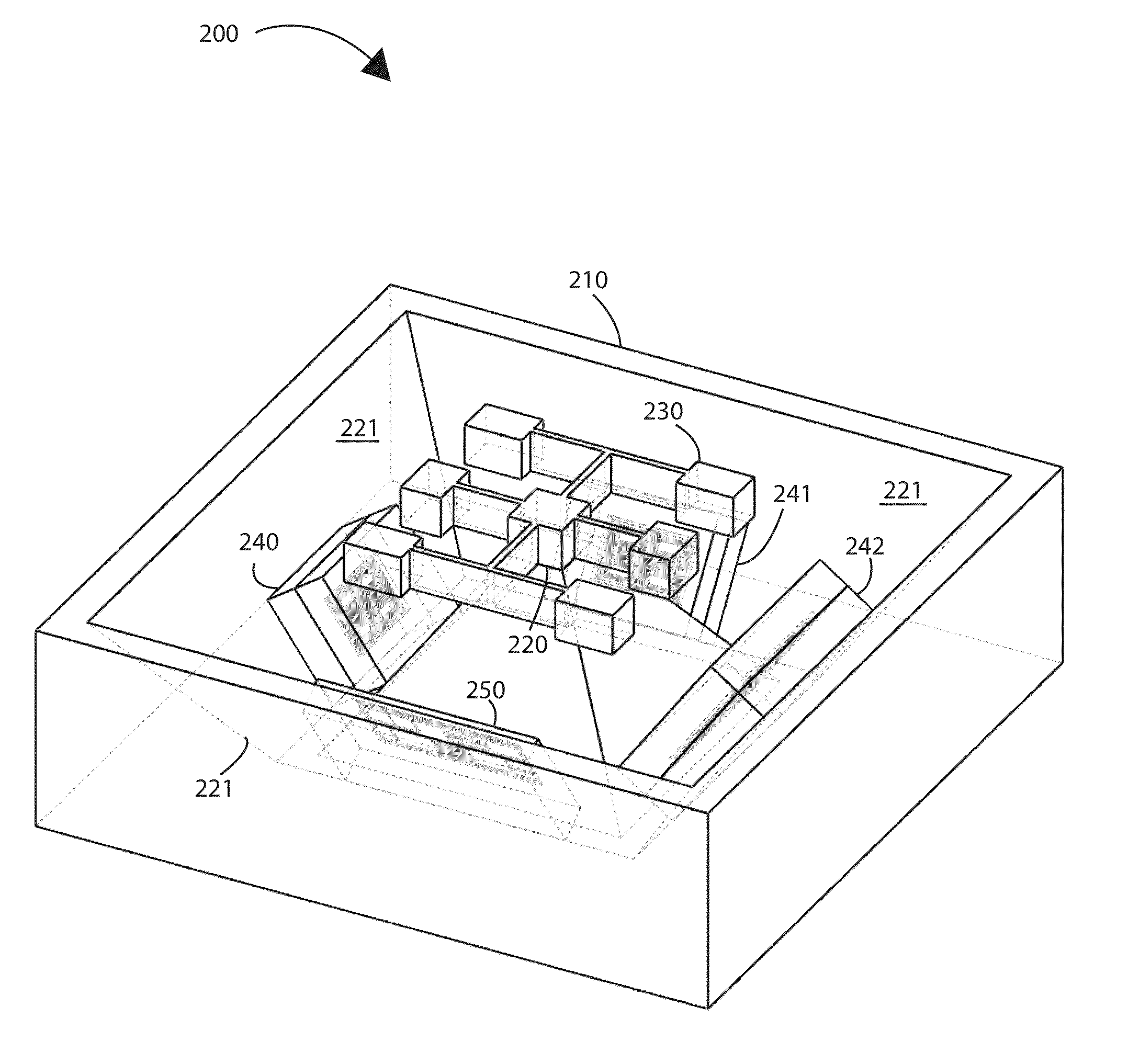
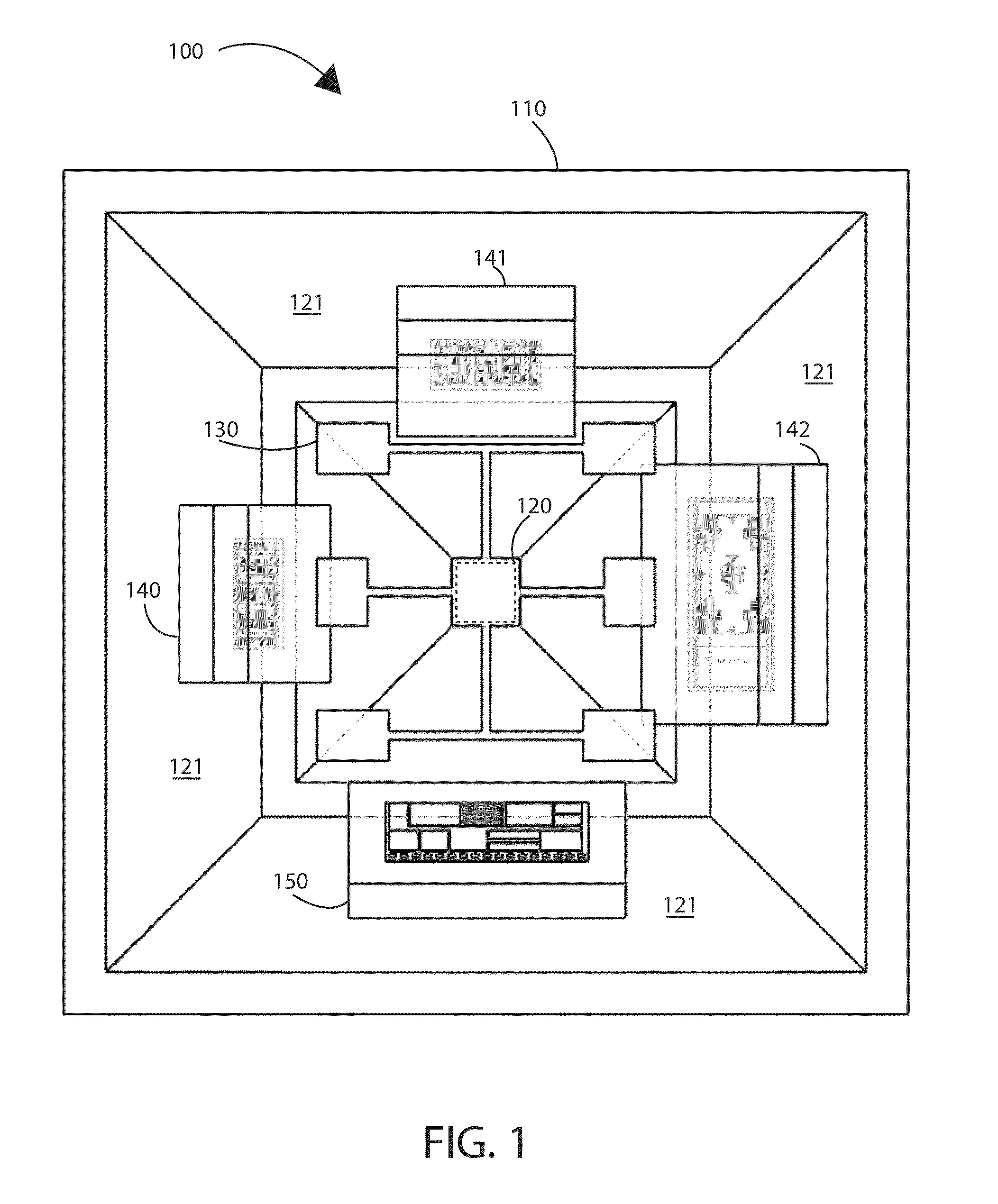
[0023]According to the present invention, techniques related generally to integrated devices and systems are provided. More particularly, the present invention provides a system and method for integrating MEMS devices with other system applications, which may be configured on at least CMOS integrated circuit devices. Merely by way of example, the MEMS devices can include at least an accelerometer, a gyroscope, a magnetic sensor, a pressure sensor, a microphone, a humidity sensor, a temperature sensor, a chemical sensor, a biosensor, an inertial sensor, and others. Additionally, the other applications include at least a sensor application or applications, system applications, and broadband applications, among others. But it will be recognized that the invention has a much broader range of applicability.

[0024]FIG. 1 is a simplified top diagram of a quartz and MEMS inertial sensing apparatus configured on crystallographic planes according to an embodiment of the present invention. This...


PUM


Abstract

An apparatus for inertial sensing. The apparatus includes a substrate member comprising a thickness of silicon. The apparatus also has a first surface region configured from a first crystallographic plane of the substrate and a second plane region configured from a second crystallographic plane of the substrate. The apparatus has a quartz inertial sensing device coupled to the first surface region, and one or more MEMS inertial sensing devices coupled to the second plane region.

Description

CROSS-REFERENCES TO RELATED APPLICATIONS[0001]The present application claims priority to and incorporates by reference, for all purposes, the following patent application: U.S. Pat. App. No. 61 / 308,941, filed Feb. 27, 2010. The present invention also incorporates by reference, for all purposes, the following co-pending patent applications related to CMOS & MEMS devices and IC fabrication methodology: U.S. patent application Ser. No. 12 / 490,067, filed Jun. 23, 2009, U.S. patent application Ser. No. 12 / 717,070, filed Mar. 3, 2010, U.S. patent application Ser. No. 12 / 945,087, filed Nov. 12, 2010, U.S. Pat. App. No. 61 / 356,467, filed Jun. 18, 2010, and U.S. patent application Ser. No. 12 / 913,440, filed Oct. 27, 2010.BACKGROUND OF THE INVENTION[0002]The present invention relates generally to integrated devices. More particularly, the present invention provides a system and method for integrating at least two different micro electro mechanical systems (MEMS), which may optionally include ...

Claims


Application Information

Patent Timeline
Patent Type & Authority Patents(United States)
IPC IPC(8): G01P1/02G01C19/56
CPCG01C19/56G01P1/02G01P1/023G01C19/5628G01C19/5769G01C19/5783H01L2224/48091H01L2924/00014
Inventor YANG, XIAO, "CHARLES"
Owner MOVELLA INC
Why Eureka
Try Eureka