Substrate processing apparatus, substrate processing method, substrate holding mechanism, and substrate holding method

a substrate processing and processing method technology, applied in lighting and heating apparatus, cleaning using liquids, lapping machines, etc., can solve the problems of affecting the overall throughput, the substrate processing apparatus in its entirety is reduced, and the plurality of polished wafers cannot be cleaned and dried simultaneously, so as to improve the overall throughput of the substrate processing operation, simple structure, and easy maintenance

Active Publication Date: 2014-08-05
EBARA CORP
View PDF72 Cites 16 Cited by
  • Summary
  • Abstract
  • Description
  • Claims
  • Application Information

AI Technical Summary

Benefits of technology

[0019]It is a third object of the present invention to provide a top ring assembly capable of responding promptly to a command for changing a pressing force against a substrate.
[0077]Further, according to the present invention, because the force of holding the substrate is generated by the vertical movements of the substrate-support members, it is not necessary to provide an electric actuator. Therefore, the substrate holding mechanism with a simple structure can be realized. The substrate holding mechanism according to the present invention can be applied to a cleaning apparatus for cleaning a substrate by supplying a cleaning liquid onto the substrate while rotating the substrate and a drying apparatus for dying a substrate by rotating the substrate. Because the substrate holding mechanism according to the present invention has a simple structure and is lightweight, a rotational load on the rotating assembly can be reduced, and therefore a long life of the substrate holding mechanism can be realized. Furthermore, the substrate holding mechanism according to the present invention has an advantage that a small amount of cleaning liquid is scattered around.

Problems solved by technology

Since the substrate processing apparatus has a variety of processing sections including a polishing section and a cleaning section, a processing delay in each processing section results in a decrease in the throughput of the substrate processing apparatus in its entirety.
Consequently, plural polished wafers cannot be cleaned and dried simultaneously.
Moreover, of plural processes on the cleaning line (e.g., a primary cleaning process, a secondary cleaning process, and a drying process), the slowest process becomes a rate-limiting step in all processes and thus decides a processing time (i.e., throughput) of all processes.
Further, wafer transferring operations between the top ring and the transfer mechanism can also affect the overall throughput.
In this manner, since the horizontal movement and the vertical movement of the wafer are performed by the linear transporter and the pusher separately, a long time is needed in transferring the wafer.
Consequently, the wafer transfer mechanism has complicated structure as a whole and entails a lot of accompanying wires and pipes to be provided.
Moreover, if the transfer mechanism breaks down, it is necessary to access the wafer-transfer position for repair, and this can make it difficult to restore the transfer mechanism.
A long downtime of the substrate processing apparatus as a result of a failure and maintenance thereof leads to an increase in cost for processing a wafer.
A top ring assembly, including the top ring and the top ring head, is relatively long and heavy.
Therefore, the top ring assembly may present disadvantages in maintenance thereof.
This arrangement entails a long distance between the pressure adjuster and the top ring and may cause a delay in an actual change in the pressing force in response to a command for changing the pressing force against the substrate.
This structure may present a problem that a flow rate of the pure water in one polishing unit becomes unstable as a result of use of the pure water in the other.

Method used


Image

  • Substrate processing apparatus, substrate processing method, substrate holding mechanism, and substrate holding method
  • Substrate processing apparatus, substrate processing method, substrate holding mechanism, and substrate holding method
  • Substrate processing apparatus, substrate processing method, substrate holding mechanism, and substrate holding method

Examples


Embodiment Construction

[0140]Embodiments of the present invention will be described below with reference to the drawings. Identical or corresponding elements will be denoted by identical reference numerals and repetitive descriptions thereof will be omitted.

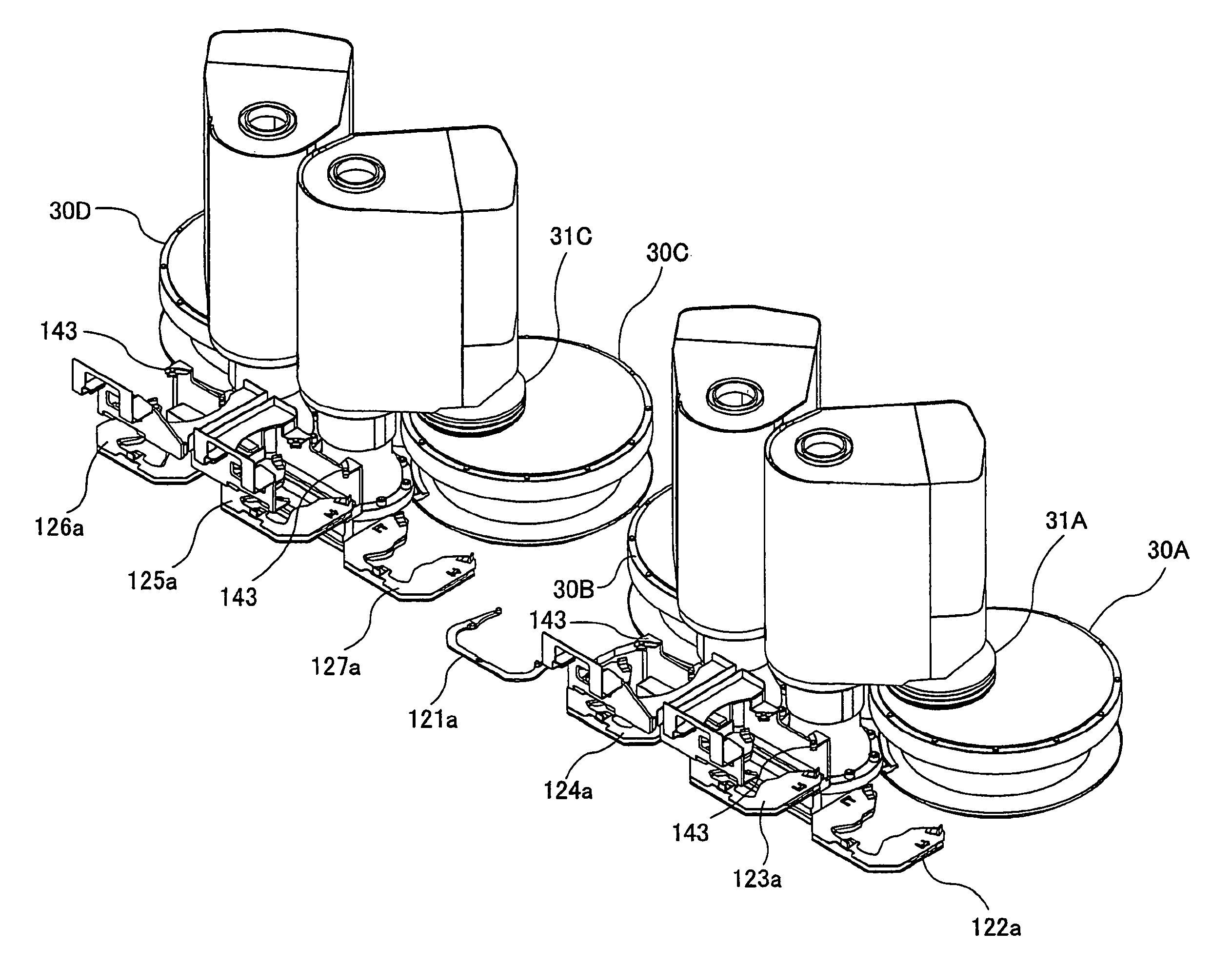
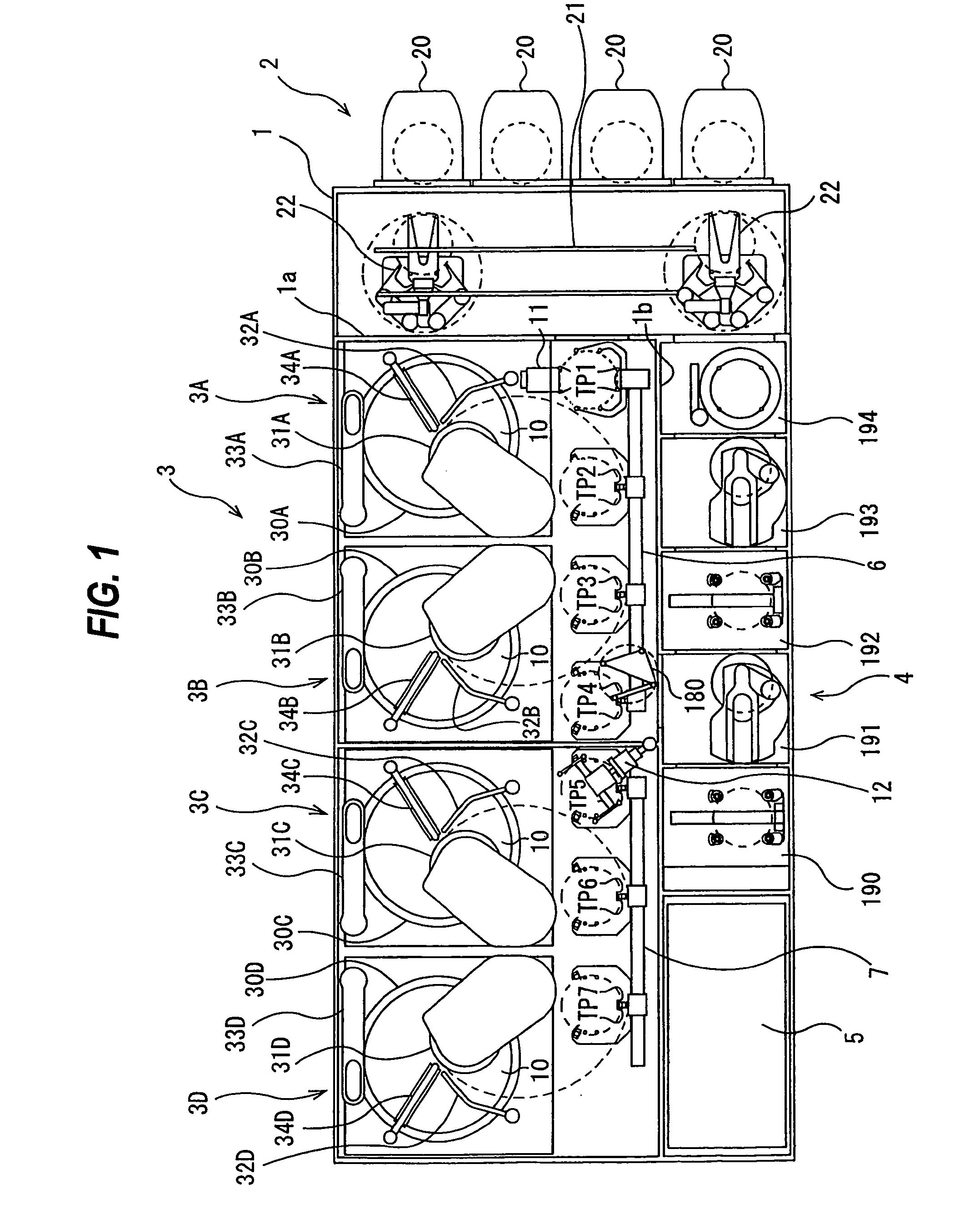
[0141]FIG. 1 is a plan view showing a whole arrangement of a substrate processing apparatus according to an embodiment of the present invention. As shown in FIG. 1, the substrate processing apparatus has a housing 1 in a rectangular shape. An interior space of the housing 1 is divided into a loading-unloading section 2, a polishing section 3, and a cleaning section 4 by partitions 1a and 1b. The loading-unloading section 2, the polishing section 3, and the cleaning section 4 are assembled independently and each section is provided with an independent gas evacuation system. The substrate processing apparatus further includes a controller 5 for controlling substrate processing operations.

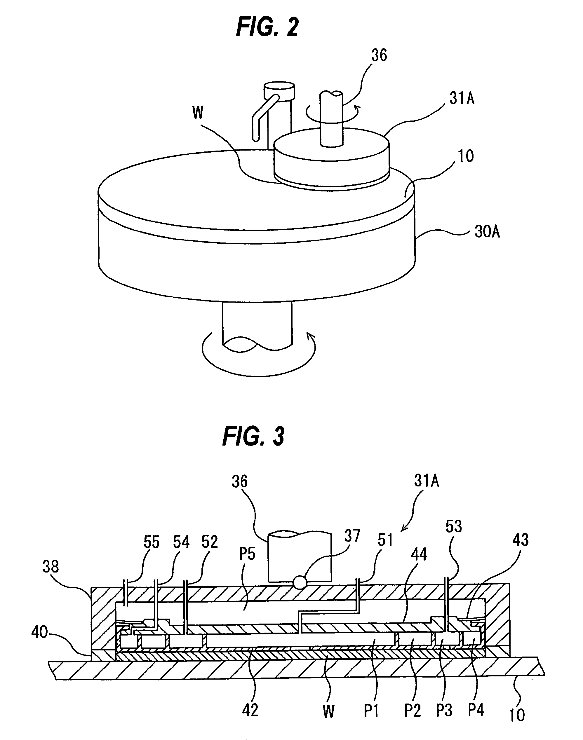
[0142]The loading-unloading section 2 has two or more (four in this...


PUM

PropertyMeasurementUnit
rotatable angleaaaaaaaaaa
angleaaaaaaaaaa
angleaaaaaaaaaa

Abstract

An apparatus for processing a substrate is disclosed. The apparatus includes a polishing section configured to polish a substrate, a transfer mechanism configured to transfer the substrate, and a cleaning section configured to clean and dry the polished substrate. The cleaning section has plural cleaning lines for cleaning plural substrates. The plural cleaning lines have plural cleaning modules and plural transfer robots for transferring the substrates.

Description

BACKGROUND OF THE INVENTION[0001]1. Field of the Invention[0002]The present invention relates to a substrate processing apparatus and a substrate processing method, and more particularly to a substrate processing apparatus and a substrate processing method for use in polishing a substrate, such as a semiconductor wafer, to provide a planarized surface of the substrate.[0003]The present invention also relates to a substrate holding mechanism and a substrate holding method, and more particularly to a substrate holding mechanism suitable for use in a cleaning apparatus and a drying apparatus for a substrate such as a semiconductor wafer.[0004]The present invention also relates to units and several types of components and mechanisms for use in a substrate processing apparatus.[0005]2. Description of the Related Art[0006]The trend of a semiconductor device in recent years has been a highly integrated structure, which entails finer interconnects of a circuit and a smaller distance between...

Claims


Application Information

Patent Timeline
Patent Type & Authority Patents(United States)
IPC IPC(8): B24B51/00
CPCH01L21/67754H01L21/30625B24B37/345H01L21/67219H01L21/67742Y10T137/8593H01L21/67739Y10T137/0318
Inventor MIYAZAKI, MITSURUKATSUOKA, SEIJIMATSUDA, NAOKIKUNISAWA, JUNJIKOBAYASHI, KENICHISOTOZAKI, HIROSHISHINOZAKI, HIROYUKINABEYA, OSAMUMORISAWA, SHINYAOGAWA, TAKAHIROMAKINO, NATSUKI
Owner EBARA CORP
Why Eureka
Try Eureka