
Phase change memory having stabilized microstructure and manufacturing method

a phase change memory and microstructure technology, applied in the field of memory devices, can solve the problems of increasing the complexity of control circuitry needed to operate the device, endurance of the dimension phase change device, and the inability to stabilize so as to improve the stability of the resistance in the set state

Active Publication Date: 2014-08-19
MACRONIX INT CO LTD
View PDF407 Cites 8 Cited by
  • Summary
  • Abstract
  • Description
  • Claims
  • Application Information

AI Technical Summary

Benefits of technology

The patent text describes a method for improving the stability of resistance in a memory device by applying a forming current in longer pulses than the set / reset pulses used during operation. The forming current can be a single pulse or multiple pulses with a duration of more than 0.5 milliseconds. The method has been tested with silicon oxide doped for GexSbyTez, and the resulting device shows improved stability of resistance in the set state. However, the method can also be extended to other chalcogenide materials, including materials with dielectric and active doping components.

Problems solved by technology

One problem with very small dimension phase change devices involves endurance.
This drift can cause problems with reliability and increase in complexity of control circuitry needed to operate the devices.
One result of these problems is that the sensing circuitry required on the devices must handle wider ranges of resistance for each of the memory states, which typically results in lower speed operation.
Also, the set and reset processes must account for varying bulk conditions of the memory cells even within a single memory state, which typically results uneven set and reset speeds across the array.

Method used


Image

  • Phase change memory having stabilized microstructure and manufacturing method
  • Phase change memory having stabilized microstructure and manufacturing method
  • Phase change memory having stabilized microstructure and manufacturing method

Examples


Embodiment Construction

[0039]A detailed description of embodiments of the present invention is provided with reference to FIGS. 1-28.

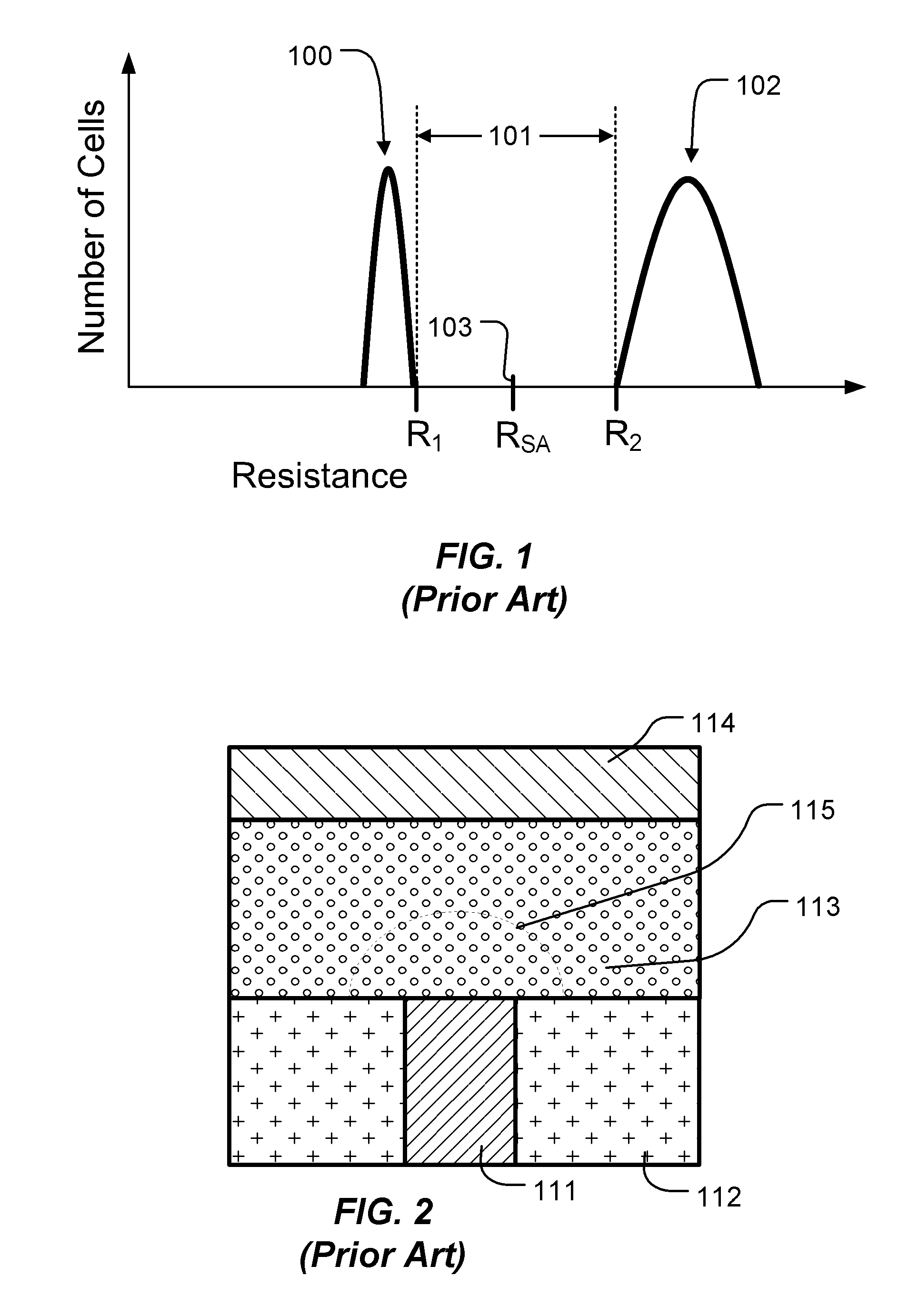
[0040]In phase change memory, data is stored by causing transitions in an active region of the phase change material between amorphous and crystalline phases, which have significantly different resistances. FIG. 1 is a graph of resistance distributions for memory states in memory cells storing a single bit of data, including a low resistance set (programmed) state 100 corresponding to a primarily crystalline phase in the active region of the cell, and a high resistance reset (erased) state 102 corresponding to a primarily amorphous phase in the active region of the cell. For reliable operation, the resistance distributions must have non-overlapping resistance ranges.

[0041]The difference between the highest resistance R1 of the set state 100 and the lowest resistance R2 of the reset state 102 defines a read margin 101 used to distinguish cells in the set state 100 from those ...


PUM


Abstract

A memory device having a phase change material element with a modified stoichiometry in the active region does not exhibit drift in set state resistance. A method for manufacturing the memory device includes first manufacturing an integrated circuit including an array of phase change memory cells with bodies of phase change material having a bulk stoichiometry; and then applying forming current to the phase change memory cells in the array to change the bulk stoichiometry in active regions of the bodies of phase change material to the modified stoichiometry, without disturbing the bulk stoichiometry outside the active regions. The bulk stoichiometry is characterized by stability under the thermodynamic conditions outside the active region, while the modified stoichiometry is characterized by stability under the thermodynamic conditions inside the active region.

Description

PARTIES TO A JOINT RESEARCH AGREEMENT[0001]International Business Machines Corporation, a New York corporation, and Macronix International Corporation, Ltd., a Taiwan corporation, are parties to a Joint Research Agreement.BACKGROUND OF THE INVENTION[0002]1. Field of the Invention[0003]The present invention relates to memory devices based on chalcogenide materials, and methods for manufacturing such devices.[0004]2. Description of Related Art[0005]Phase change based memory materials, like chalcogenide based materials and similar materials, can be caused to change phase between an amorphous state and a crystalline state by application of electrical current at levels suitable for implementation in integrated circuits. The generally amorphous state is characterized by higher electrical resistivity than the generally crystalline state, which can be readily sensed to indicate data. These properties have generated interest in using programmable resistive material to form nonvolatile memory...

Claims


Application Information

Patent Timeline
Patent Type & Authority Patents(United States)
IPC IPC(8): H01L47/00H10N80/00
CPCH01L45/06H01L45/1226H01L45/1233H01L45/1246H01L45/144H01L45/1625H01L45/1641G11C2013/0083G11C13/0069H10N70/828H10N70/823H10N70/231H10N70/041H10N70/026H10N70/8828H10N70/826
Inventor LEE, MING-HSIU
Owner MACRONIX INT CO LTD
Learn More