Single clock distribution network for multi-phase clock integrated circuits

a technology of integrated circuits and single clocks, applied in the field of digital circuits, can solve the problems of increasing the difficulty of clock distribution in high-performance microprocessors and other ics, affecting the synchronization of independent clock phases, and requiring the provision of multiple clock distribution networks for each phas

Active Publication Date: 2014-09-30
IRONWOOD CYBER INC
View PDF10 Cites 2 Cited by
  • Summary
  • Abstract
  • Description
  • Claims
  • Application Information

AI Technical Summary

Benefits of technology

[0016]The present invention provides a single global clock distribution network for a Multiple-Valued Logic (MVL) clock signal in combination with new level-sensitive latches designed to be transparent for a specific portion of the global MVL clock signal. This approach allows for the use of conventional binary logic fabrication technology since the only MVL components required are the global clock generator and a modified literal selection gate that can be implemented as small analog circuits. A purely binary implementation approach is also described where the MVL clock signal is replaced by a binary encoded signal and the phase-sensitive latches are augmented by including a binary decoder function that allows for implementation of the method using commercially available FPGA devices or a standard cell library containing only binary logic cells.

Problems solved by technology

While multi-phase clocking has the advantage of retaining high-performance while relaxing timing constraints within each subcircuit phase domain, the significant disadvantage is that multiple clock distribution networks must be provided for each phase clock instead of a single global clock distribution network.
The increase in clock uncertainties due to higher clock frequencies has made designing clock distributions in high-performance microprocessors and other ICs increasingly difficult.
Difficulties also arise in maintaining synchronization among the independent clock phases.
However, the transparent nature of latches increases the difficulty in meeting timing criteria as compared to the use of edge-sensitive circuits.
As is apparent from the foregoing discussion, multi-phase clock distribution systems require a significant amount of resources in terms of area and power dissipation.

Method used


Image

  • Single clock distribution network for multi-phase clock integrated circuits
  • Single clock distribution network for multi-phase clock integrated circuits
  • Single clock distribution network for multi-phase clock integrated circuits

Examples


Embodiment Construction

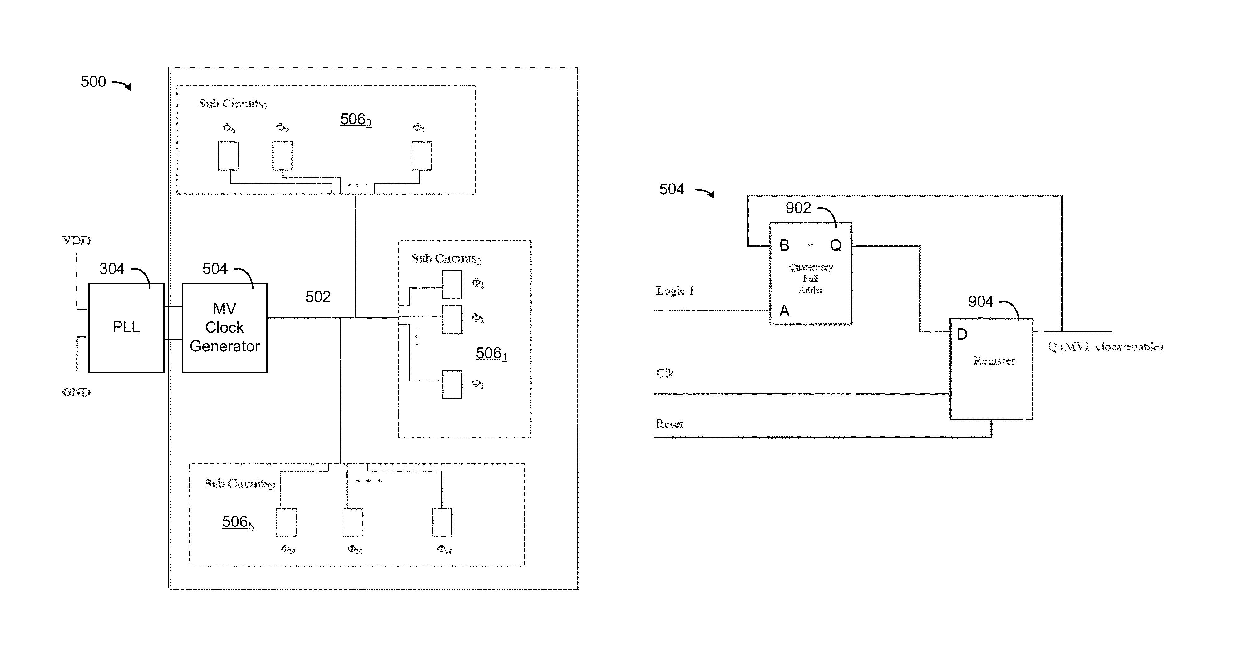
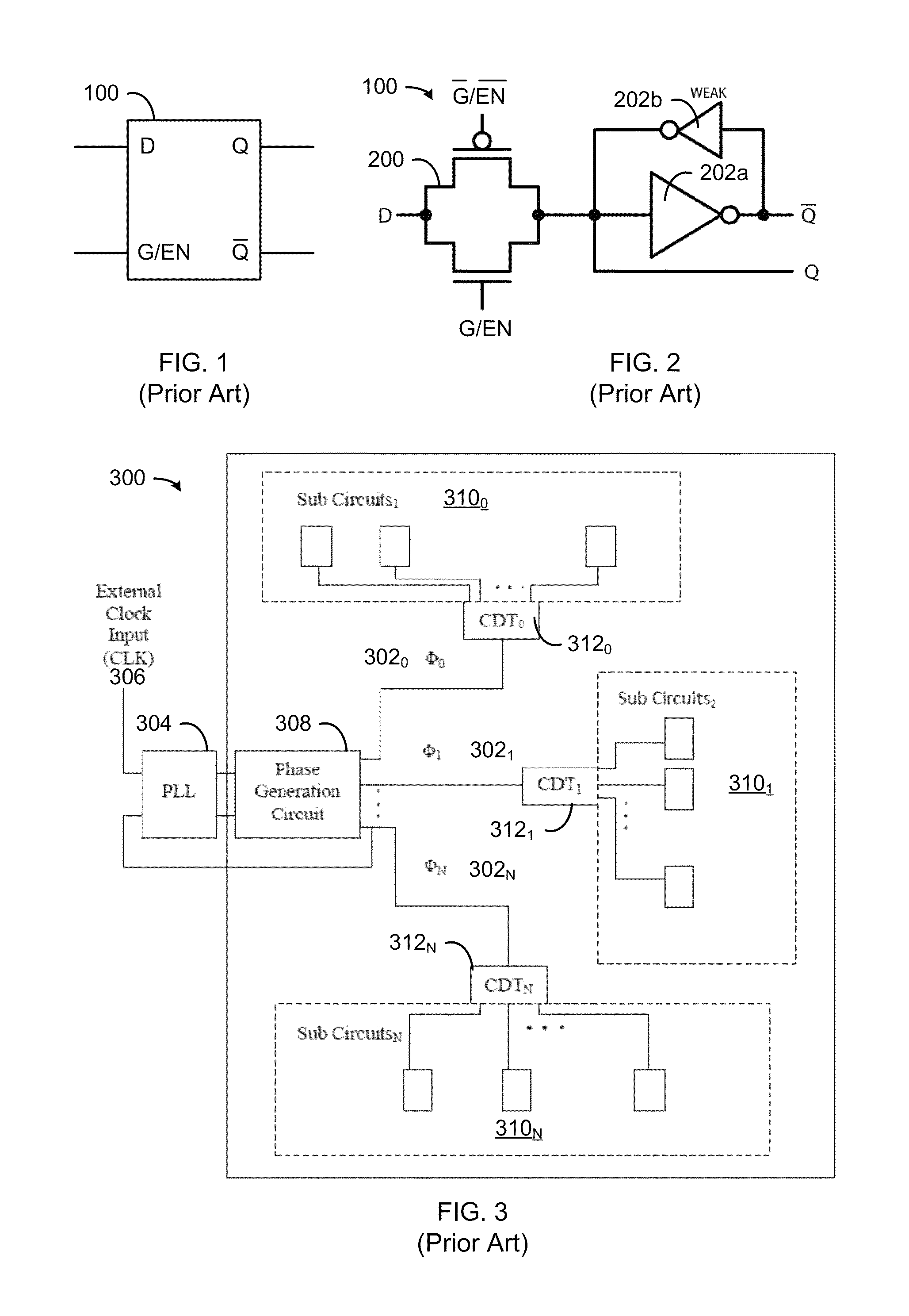
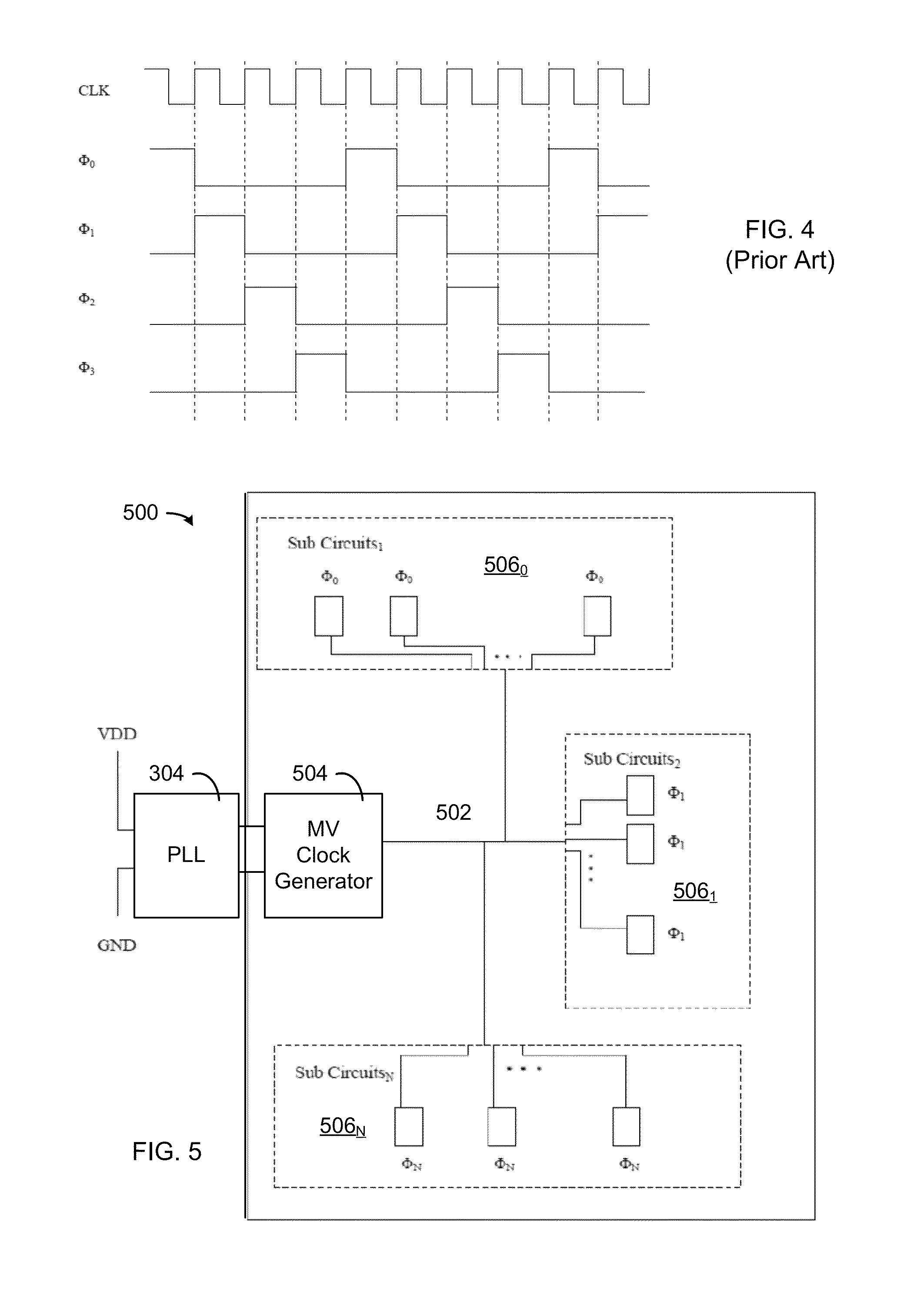
[0046]While the making and using of various embodiments of the present invention are discussed in detail below, it should be appreciated that the present invention provides many applicable inventive concepts that can be embodied in a wide variety of specific contexts. The specific embodiments discussed herein are merely illustrative of specific ways to make and use the invention and do not delimit the scope of the invention. The discussion herein relates primarily to a four-valued voltage-mode quaternary clock signal (i.e. four logic levels—logic 0, logic 1, logic 2 and logic 3), but it will be understood that the concepts of the present invention are applicable to any Multiple-Valued Logic (MVL) (three or more value) system. Note also that the logic levels can implemented as positive or negative voltages depending on the architecture of the integrated circuit.

[0047]The MVL-based method described herein implements the strategy of a multi-phase clocking architecture but utilizes a si...


PUM


Abstract

A multi-valued logic (MVL) circuit includes a MVL clock generator that generates a MVL clock signal having three or more ith MVL levels, a single MVL clock signal distribution network connected to the MVL clock generator, and three or more ith MVL selection circuits connected to the single MVL clock signal distribution network where i=0 to N and N>=3. Each ith MVL selection circuit corresponds to a specified ith MVL level. The ith MVL selection circuit outputs an ith binary clock signal having: (a) a first logic level whenever the MVL clock signal is equal to the ith MVL level and the ith data input receives the first logic level, (b) a second logic level whenever the MVL clock signal is equal to the ith MVL level and the ith data input receives the second logic level, and (c) a previous logic level of the ith binary clock signal whenever the MVL clock signal is not equal to the ith MVL level.

Description

CROSS REFERENCE TO RELATED APPLICATIONS[0001]This patent application is a non-provisional patent application of U.S. provisional patent application 61 / 599,598 filed on Feb. 16, 2012, which is hereby incorporated by reference in their entirety.FIELD OF THE INVENTION[0002]The present invention relates generally to the field of digital circuitry and, more particularly, to a single clock distribution network for multi-phase clock integrated circuits.BACKGROUND OF THE INVENTION[0003]Increasing the performance of Integrated Circuits (ICs) is of paramount concern to support advances in technology. Many techniques are employed for increasing performance, ranging from new and improved fabrication technology to advances in design techniques. One design approach is that of partitioning a globally clocked synchronous logic circuit into disjoint subcircuits referred to as ‘phases.’ Each phase then utilizes a private clock distribution network with a substantially reduced clock frequency. However...

Claims


Application Information

Patent Timeline
Patent Type & Authority Patents(United States)
IPC IPC(8): H03K19/00H03L7/00G06F1/04G06F1/10H03K19/096
CPCH03K19/096G06F1/10
Inventor THORNTON, MITCHELL AARONMENON, ROHIT
Owner IRONWOOD CYBER INC
Why Eureka
Try Eureka