Simultaneous topographic and elemental chemical and magnetic contrast in scanning tunneling microscopy

a scanning tunneling and magnetic contrast technology, applied in the field of scanning tunneling microscopes, can solve the problems of inability to render adequate chemical imaging and limited spatial resolution of sxstm, and achieve the effect of increasing spatial resolution and significantly increasing the sensitivity of spm

Active Publication Date: 2014-09-30
UCHICAGO ARGONNE LLC
View PDF1 Cites 0 Cited by
  • Summary
  • Abstract
  • Description
  • Claims
  • Application Information

AI Technical Summary

Problems solved by technology

Without the filter topography and chemical contrasts would be entangled, rendering adequate chemical imaging impossible; 2) Nanofabricated coaxial multilayer tips with nanoscale conducting apex: The larger the area illuminated by the X-rays, the larger the number of photoelectrons ejected from the sample.
Therefore, the spatial resolution of SXSTM would be limited by the size of the X-ray beam.

Method used


Image

  • Simultaneous topographic and elemental chemical and magnetic contrast in scanning tunneling microscopy
  • Simultaneous topographic and elemental chemical and magnetic contrast in scanning tunneling microscopy
  • Simultaneous topographic and elemental chemical and magnetic contrast in scanning tunneling microscopy

Examples


example 1

Smart Tip Rotator: Complete Components List

[0051]The following sets forth a component list for the NanoRotator 260 described hereinbefore.

Microprocessor:

1 Arduino Pro Mini, 3.3V

1 FTOI Basic Breakout, 3.3V (allows powering and communication with computer through USB)

1 USB Mini-B Cable, 6 foot

Transistors:

1 bipolar, NPN, type 2N2222

Resistors:

1 metal film resistor, 7.5 Ohm, 0.6 W

1 metal film resistor, 65 Ohm, 0.4 W

Capacitors (Ceramic):

1,220 microfarad

Diode:

1 Standard, 1 A, 50V, type 1N4001GP-E3

LED's:

1 green LED, SMD, 50 mcd, 2V, 20 mA, 130 degrees viewing angle.

1 red LED, SMD, 50 mcd, 2V, 20 mA, 130 degrees viewing angle.

Battery:

2 Lithium button battery type CR2016, 3V.

1 battery holder, 20 mm coin cell, surface mount

Screws (Bottom Electrode-Transport Tip Characterization):

Metric head slotted machine screws, 18-8 SS, 5 to 10 mm long.

Adapter:

1 dovetail stage adapter for SEISS.LEO SEM and FIB

Bearings / Gears / Motor:

2 hydro-dynamic pressure bearing, 1.5 mm bore, 4 mm 00, 2 mm wide

3 Miter gear,...

example 2

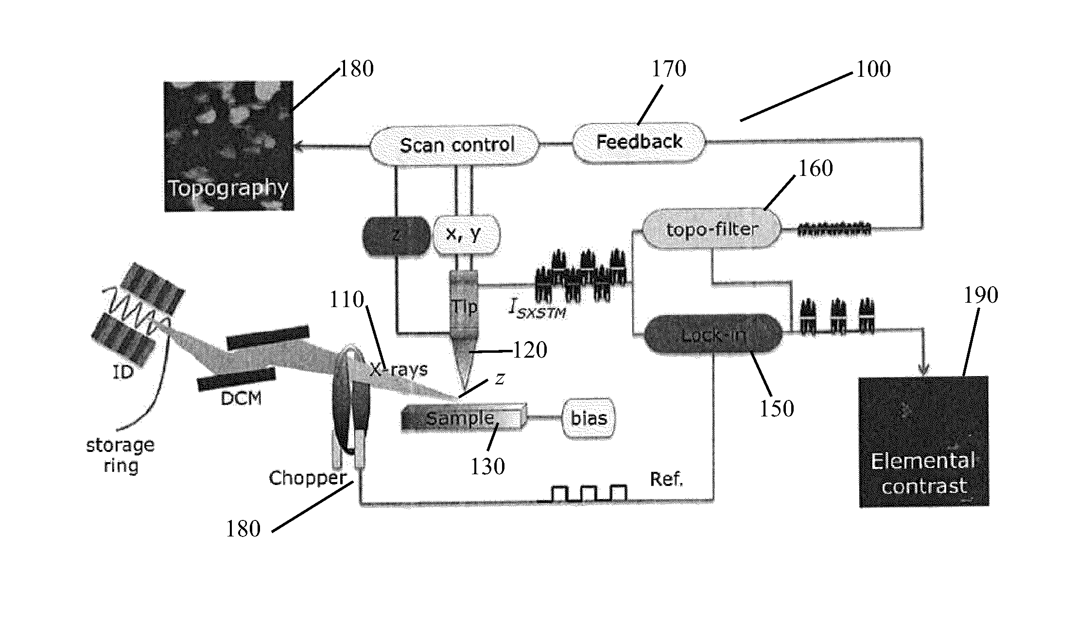
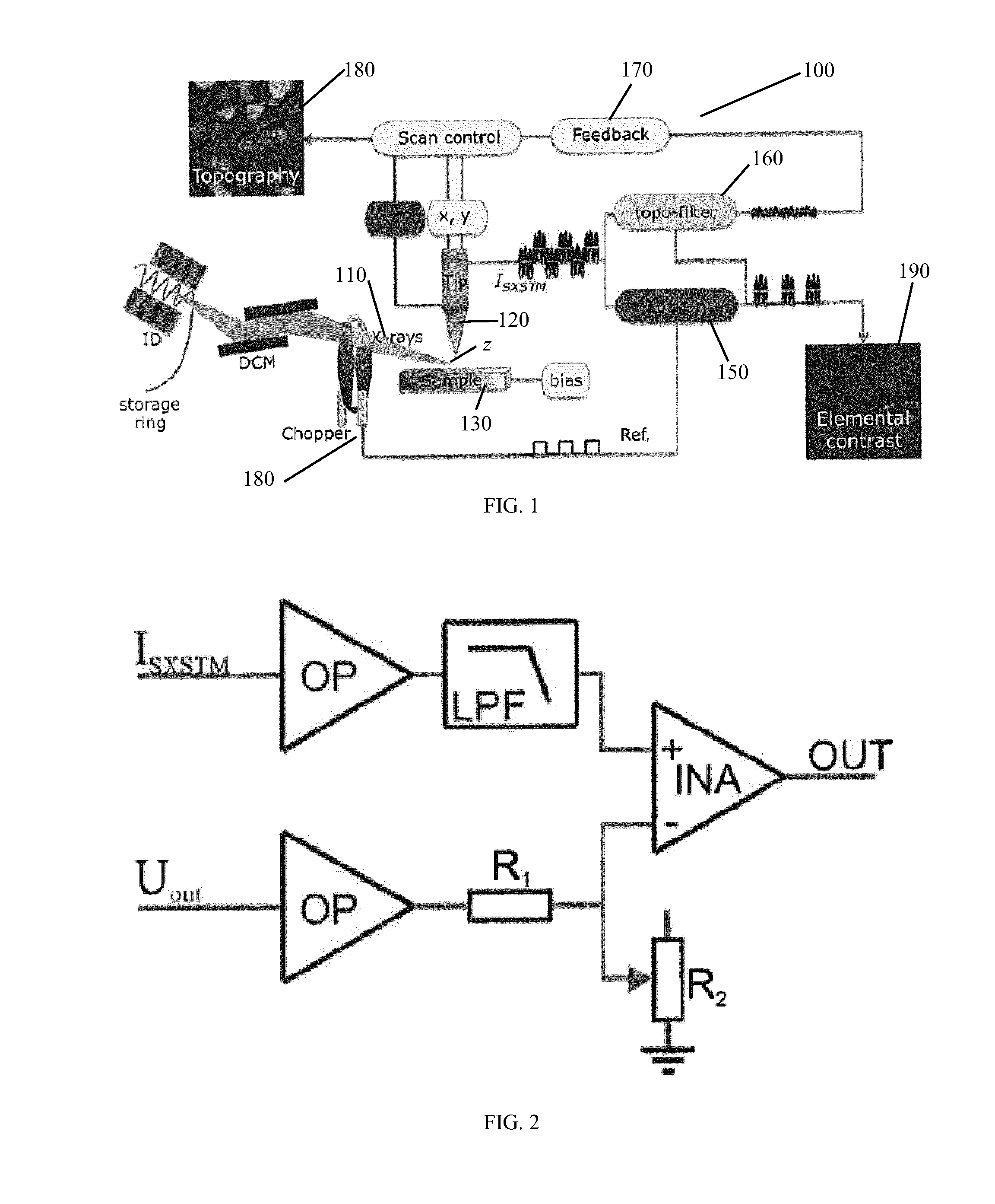
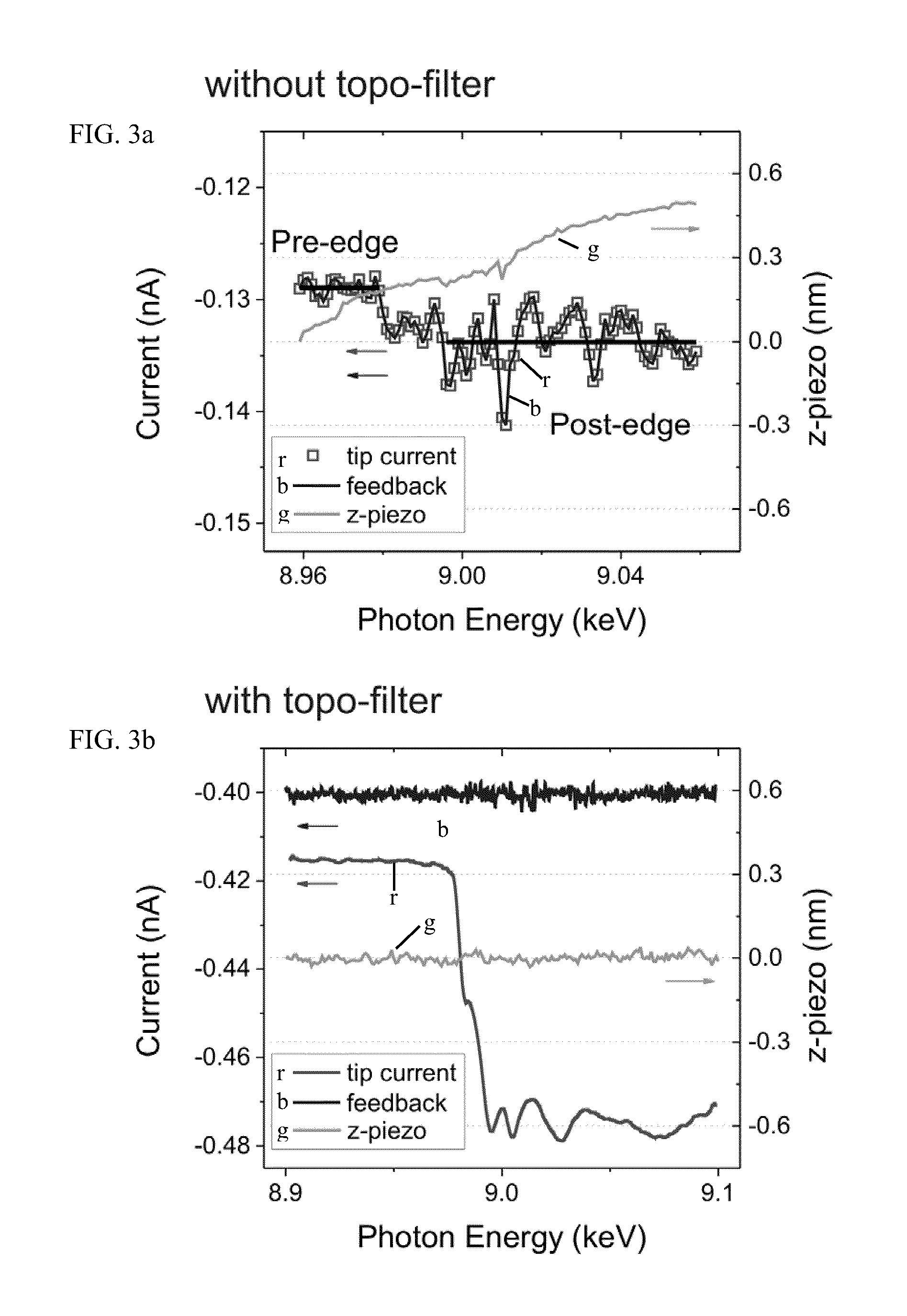
[0052]The functionality of the invention has been verified in both (1) the spectroscopy mode (ramping the photon energy while the tip tunnels over a fixed sample location) and (2) imaging mode (rastering the tip over the sample surface while the X-ray energy is fixed to a particular absorption energy of interest). The three components (topo-filter, coaxial smart tip, and NANORotator) have been utilized to achieve simultaneous topography and chemical imaging using the setup shown in FIG. 1. One example result is shown in FIGS. 6a and 6b, where both the topographic surface (FIG. 6a) and the chemical image (FIG. 6b) of the sample surface 130 have been obtained (Co in alumina clusters). The typical scan speed is about 5 ˜s per pixel. FIGS. 3a and 3b show a comparison of spectroscopy scans of the photon energy while the tip 130 (200) is tunneling over a Cu(111) surface. The X-ray illumination with a photon energy around the Cu K edge on the sample gives rise to an absorption spectrum tha...


PUM


Abstract

A method and system for performing simultaneous topographic and elemental chemical and magnetic contrast analysis in a scanning, tunneling microscope. The method and system also includes nanofabricated coaxial multilayer tips with a nanoscale conducting apex and a programmable in-situ nanomanipulator to fabricate these tips and also to rotate tips controllably.

Description

[0001]This invention was made with United States government support pursuant to a contract with the following agency: U.S. Department of Energy Contract No. DE-ACO2-06CH11357. The United States government has certain rights in this invention.FIELD OF THE INVENTION[0002]The invention relates generally to a scanning tunneling microscope and methods of use. More particularly the invention is related to method and system for performing simultaneous topographic and elemental chemical and magnetic contrast analysis in a scanning tunneling microscope. The method and system also includes nanofabricated coaxial multilayer tips with a nanoscale conducting apex and a programmable in-situ manipulator to fabricate these tips and also to rotate tips controllably.BACKGROUND OF THE INVENTION[0003]Advancements in material fabrication demand the tailoring of their properties to respond to immediate and future technical challenges. This implies creating materials that may not even exist naturally, or ...

Claims


Application Information

Patent Timeline
Patent Type & Authority Patents(United States)
IPC IPC(8): G01Q60/16
CPCB82Y35/00G01Q60/16G01Q60/14
Inventor ROSE, VOLKERPREISSNER, CURT A.HLA, SAW-WAIWANG, KANGKANGROSENMANN, DANIEL
Owner UCHICAGO ARGONNE LLC
Why Eureka
Try Eureka