Vertical gallium nitride-based light emitting diode and method of manufacturing the same

a technology of light-emitting diodes and vertical gallium nitride, which is applied in the direction of semiconductor/solid-state device manufacturing, electrical apparatus, semiconductor devices, etc., can solve the problems of difficult to obtain high optical output and provide noticeable increase in optical synergy, so as to reduce power consumption, improve optical output, and reduce the consumption of fossil fuels

Active Publication Date: 2014-10-14
SEOUL VIOSYS CO LTD +1
View PDF22 Cites 0 Cited by
  • Summary
  • Abstract
  • Description
  • Claims
  • Application Information

AI Technical Summary

Benefits of technology

[0009]The present disclosure provides a technology for enabling a significant improvement in optical output from a vertical GaN-based light emitting diode using an Ag-based highly reflective p-type electrode, quasi-photonic crystal, and surface roughening.
[0012]The technology according to the present disclosure using an highly reflective p-type electrode, quasi-photonic crystals and surface roughness may be immediately applied to a process of manufacturing common GaN-based light emitting diodes, and may achieve a significant improvement in optical output from the light emitting diode to bring forth the era of solid state lighting based on the GaN-based light emitting diodes as a white light source. Furthermore, the technology according to the present disclosure is an environmentally friendly technology that can reduce consumption of fossil fuels through reduced power consumption.

Problems solved by technology

When an n-type semiconductor layer has a smooth and flat surface, a considerable amount of light generated in an active layer cannot be emitted due to total internal reflection occurring at an interface between the atmosphere and a semiconductor layer, thereby making it difficult to obtain high optical output.
That is, these three schemes provide noticeable increase synergies for optical output.

Method used


Image

  • Vertical gallium nitride-based light emitting diode and method of manufacturing the same
  • Vertical gallium nitride-based light emitting diode and method of manufacturing the same
  • Vertical gallium nitride-based light emitting diode and method of manufacturing the same

Examples


Embodiment Construction

[0019]Exemplary embodiments of the present disclosure will now be described in detail with reference to the accompanying drawings. The following embodiments are given by way of illustration only so as to provide a thorough understanding of the invention to those skilled in the art and may be embodied in different forms.

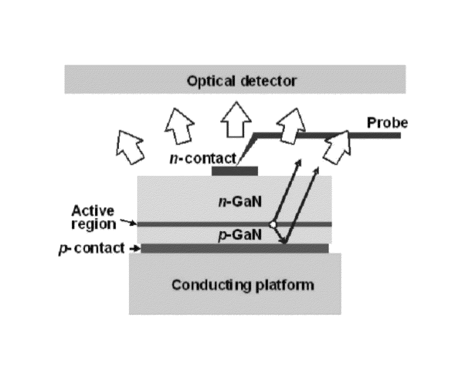
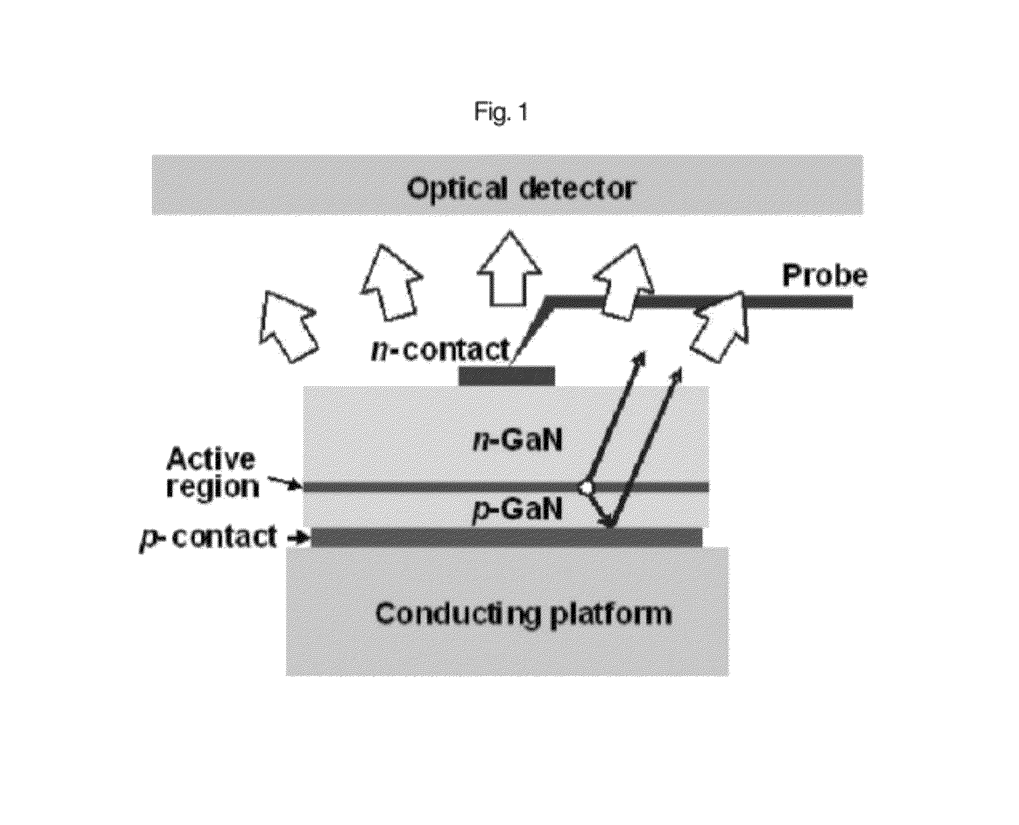
[0020]FIG. 1 is a side section view of a vertical GaN-based light emitting diode according to one exemplary embodiment of the present disclosure, diagrammatically showing an optical measurement method. The vertical GaN-based light emitting diode is fabricated by growing an epitaxial thin film of a GaN-based light emitting diode on a sapphire substrate, lifting-off the epitaxial thin film from the substrate using a laser, and then bonding the vertical GaN-based light emitting diode to a metal substrate such as a Ni, Au, Cu or Ni—Fe alloy substrate, or to a semiconductor substrate such as an Si or GaAs substrate. In this case, an existing Ni / Au electrode or highly refle...


PUM

PropertyMeasurementUnit
wavelengthaaaaaaaaaa
output wavelengthaaaaaaaaaa
reflectivityaaaaaaaaaa

Abstract

The present disclosure provides a vertical GaN-based semiconductor diode and a method of manufacturing the same. The GaN-based πi-V group semiconductor device includes a substrate, a p-type ohmic electrode layer on the substrate, a p-type GaN-based πi-V group compound semiconductor layer on the p-type ohmic electrode layer, an n-type GaN-based πi-V group compound semiconductor layer on the p-type GaN-based πi-V group compound semiconductor layer, and an n-type ohmic electrode layer on the n-type GaN-based IE-V group compound semiconductor layer. The p-type ohmic electrode layer is an Ag-based highly reflective electrode having a high reflectivity of 70% or more, and a surface of the n-type GaN-based E-V group compound semiconductor layer is subjected to at least one of a process of forming photonic crystals and a process of surface roughening.

Description

CROSS-REFERENCE TO RELATED APPLICATIONS[0001]This application is the National Stage of International Application No. PCT / KR2010 / 008403, filed on Nov. 25, 2010, which claims priority from and the benefit of Korean Patent Application No. 10-2009-0116122, filed on Nov. 27, 2009, both of which are incorporated by reference for all purposes as if fully set forth herein.BACKGROUND OF THE INVENTION[0002]1. Field of the Invention[0003]The present disclosure relates to a technology for an improvement in optical output from a vertical type gallium nitride (GaN)-based light emitting diode using an Ag-based highly reflective p-type electrode, quasi-photonic crystal, and surface roughening.[0004]2. Discussion of the Background[0005]With various advantageous features, such as high energy conversion efficiency, long operational lifespan, high directionality, low voltage operation, elimination of preheating time and complex drive circuit, high resistance to impact and vibration, GaN-based white lig...

Claims


Application Information

Patent Timeline
Patent Type & Authority Patents(United States)
IPC IPC(8): H01L33/00H01L21/00H01L31/0256H01L33/22H01L33/30
CPCH01L33/22H01L33/30H01L33/305H01L33/405H01L2933/0083
Inventor LEE, JONG, LAM
Owner SEOUL VIOSYS CO LTD
Why Eureka
Try Eureka