[0018]For a delta ADC based on the PMD architecture, in the absence of an analog signal, the single junction SQUID quantizer pulses at the carrier frequency (fcar) which is determined by the car average fluxon transport rate through the modulator. When an additional analog input signal is coupled to the quantizer loop, the timing of each output pulse gets advanced or retarded in proportion to the derivative of the analog input. This process encodes the signal derivative into SFQ pulse positions, which need to be decoded by measuring the pulse positions against a time reference. Hence the phase modulated SFQ pulse stream is passed to a phase demodulator (synchronizer), which is a clocked sampling circuit that generates a ‘1’ or a ‘0’ indicating whether or not an SFQ pulse arrived during that clock interval. Thus, the synchronizer decodes the pulse position information into numbers (single-bit in the simplest implementation, though devices with a higher number of bits may be implemented). The oversampled digital data and the corresponding clock from the synchronizer then proceed directly to the decimation filter, where it is first integrated at full speed, and then averaged further, reducing the output bandwidth and increasing the effective number of bits.
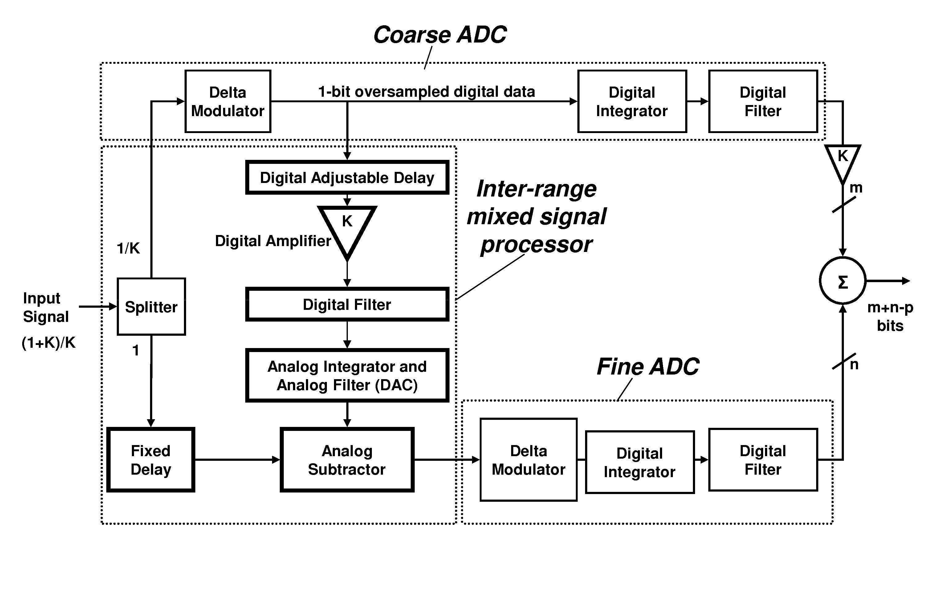
[0019]The use of two PMD ADCs in a subranging architecture is illustrated in FIG. 4C. A received signal is coupled to a coarse ADC and to a flux subtractor. The coarse ADC produces an output that represents the received signal, with quantization noise resulting from limited quantization step size. This oversampled bit sequence needs to be integrated to reconstruct a multibit digital equivalent of the input signal. This integrated output may be averaged further and read out at the decimated rate to reduce the output bandwidth and increase the effective number of bits. These bits form the most significant bits (MSB) of the subranging ADC. In order to extract the least significant bits (LSB), the oversampled 1-bit coarse ADC output is integrated in an analog integrator (based on a superconducting inductor), and then low-pass filtered to be converted back to the analog domain. Thus, this circuit is effectively a DAC with nearly ideal linearity. This analog signal is then subtracted from the input signal in a “flux subtractor”, a transformer which couples, and effectively subtracts, magnetic fields corresponding to properly synchronized and gain-adjusted representations of the input signal and analog signal from the coarse ADC, to generate a residue signal representing the error of the coarse ADC. The error signal is then digitized by the fine ADC to get the LSBs. The residue signal, being of lower amplitude than the original signal, is ideally at the full-scale range of the fine ADC, which may be another PMD ADC which is similar to the coarse ADC. The digital output of the fine ADC is combined (e.g., summed) with that of the coarse ADC to yield a digital output with a larger dynamic range (a greater effective number of bits). The output significance of the fine ADC may overlap with the lower bits of the multibit representation of the coarse ADC, permitting compensation for various errors.
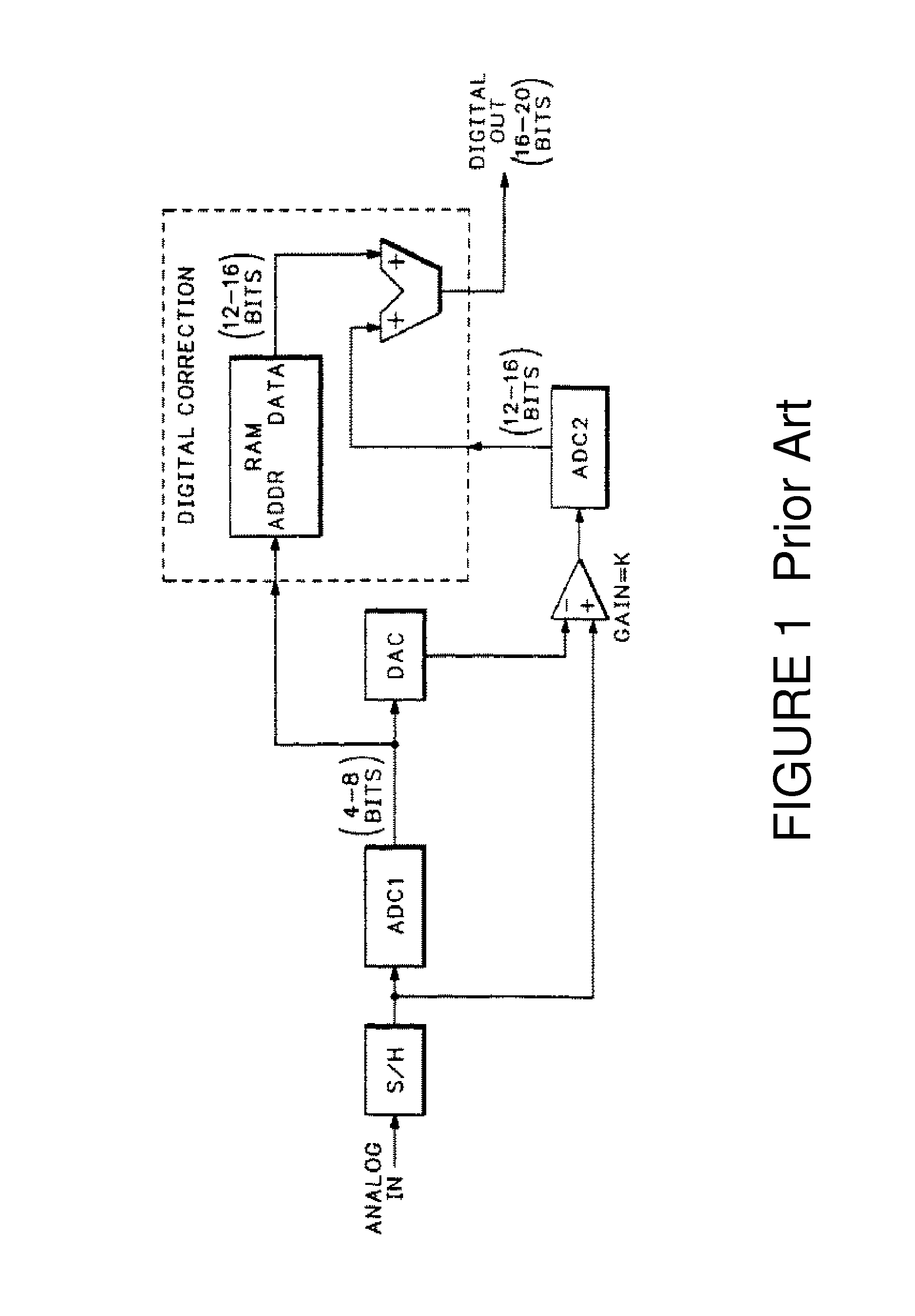
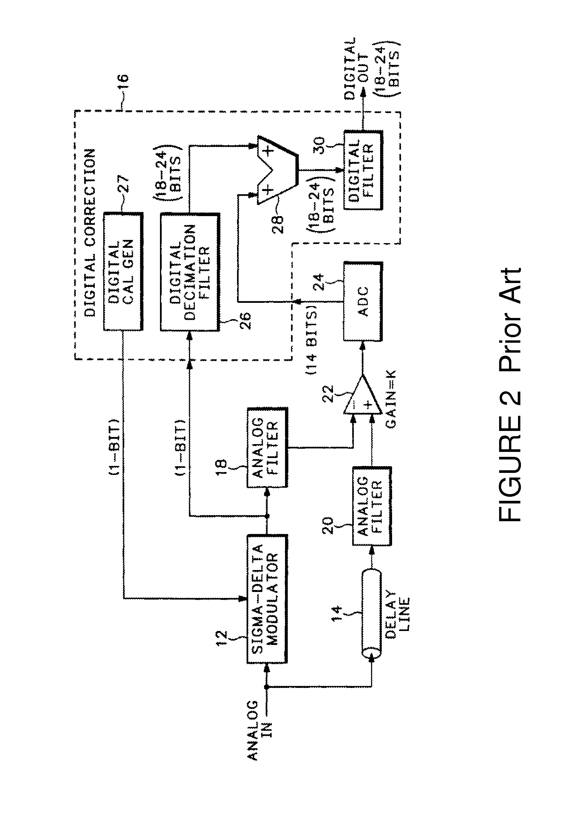
[0020]The design of FIG. 4C avoids the need for an amplifier at the output of the flux subtractor. Rather than amplifying the difference, as proposed in the embodiments according to FIGS. 1 and 2, instead this design couples a small fraction of the input signal to the coarse ADC, and amplifies the output of the coarse ADC by a factor K to restore the signal component to the same value as the remaining fraction of the input signal. Given the fact that the combination of the coarse ADC and DAC in superconductor technology conserves magnetic flux, these two scalings should permit accurate cancellation of the coarse signal in the flux subtractor. If one assumes that the fine ADC and the coarse ADC have the same sensitivity, the factor K corresponds to the additional dynamic range that the subranging ADC can ideally achieve. For example, if K=64, this corresponds to up to an additional 6 bits of precision. Alternatively, if the fine ADC is intrinsically more sensitive than the coarse ADC, additional precision may be obtained with a reduced factor of K.
[0022]The inter-range circuitry that integrates the coarse and the fine ADC performs multiple signal processing functions in the digital and in the analog domains. One embodiment of this inter-range mixed-signal processor incorporates the functions of linear amplification, integration, carrier subtraction, signal subtraction, and filtering together in a single integrated device. In another preferred embodiment of the invention, the fine ADC may have a different optimized design than the coarse ADC. For example, the fine ADC may be substantially more sensitive than the coarse ADC, which would enable increased dynamic range with a significantly reduced value of K. Alternatively, the fine ADC may comprise a sigma-delta ADC, which is less sensitive to high frequency noise, and hence relaxes the requirements placed on the filter in the inter-range mixed-signal processor (see FIG. 5). Functional simulations of several subranging ADC configurations are presented, and show improvement of up to 35 dB in SNR over a single-stage superconducting ADC. A similar improvement of spur-free dynamic range (SFDR) is also expected since the harmonics and inter-modulation distortion produced by the coarse ADC appear in the residue and are treated the same way as the quantization error. These distortions will be substantially cancelled in the final output combining the coarse and the fine ADC outputs.
[0036]At least one of the fine and coarse analog-to-digital converters may comprise a digital filter. The digital filter may comprise a digital integrator. The digital filter may comprise a decimator that reduces the output sampling rate.