
Field device and method of operating high voltage semiconductor device applied with the same

a field device and high voltage technology, applied in the field of field devices and methods of operating high voltage (hv) semiconductor devices, can solve the problems of hv-well isolation failure, increased difficulty in channel reverse of hv-well under hv operation, limited maximum operating voltage, etc., and achieves the effect of increasing cost and device area, and effectively improving the threshold voltage (vth) of field devices

Active Publication Date: 2014-11-25
MACRONIX INT CO LTD
View PDF9 Cites 2 Cited by
  • Summary
  • Abstract
  • Description
  • Claims
  • Application Information

AI Technical Summary

Benefits of technology

[0007]The disclosure relates to a field device and method of operating high voltage (HV) semiconductor device having the field device. In the present disclosure, the threshold voltage (Vth) of field device is effectively improved without increasing cost and device area, so as to avoid the field device turned on when the HV semiconductor device is under high voltage operation.

Problems solved by technology

It means that when MOSFETs is under high voltage operation, maximum operating voltage is limited by turned on threshold voltage (Vth) of parasitic field devices which might be lower than the breakdown voltage of MOSFETs.
However, this method requires largest area for pad and has risks to cause HV-well isolation failure.
Another method to avoid inducing parasitic field transistor from being turned on is increasing the thickness of oxide (ILD or IMD) on the HV-well, thereby raising the difficulty for channel reverse of HV-well under HV operation.
However, this method requires longer time for growing oxide, which needs extra thermal budget, and the heat accumulation might have considerable effect on other components of the HV semiconductor device.

Method used


Image

  • Field device and method of operating high voltage semiconductor device applied with the same
  • Field device and method of operating high voltage semiconductor device applied with the same
  • Field device and method of operating high voltage semiconductor device applied with the same

Examples


first embodiment

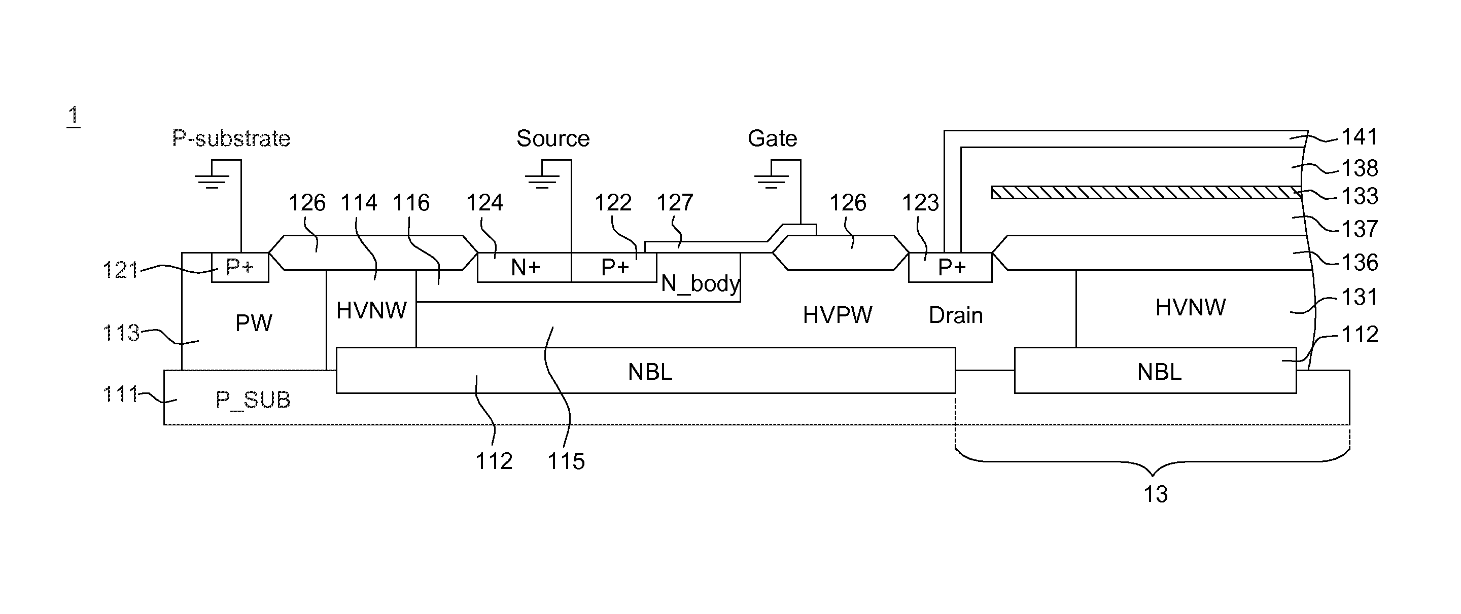
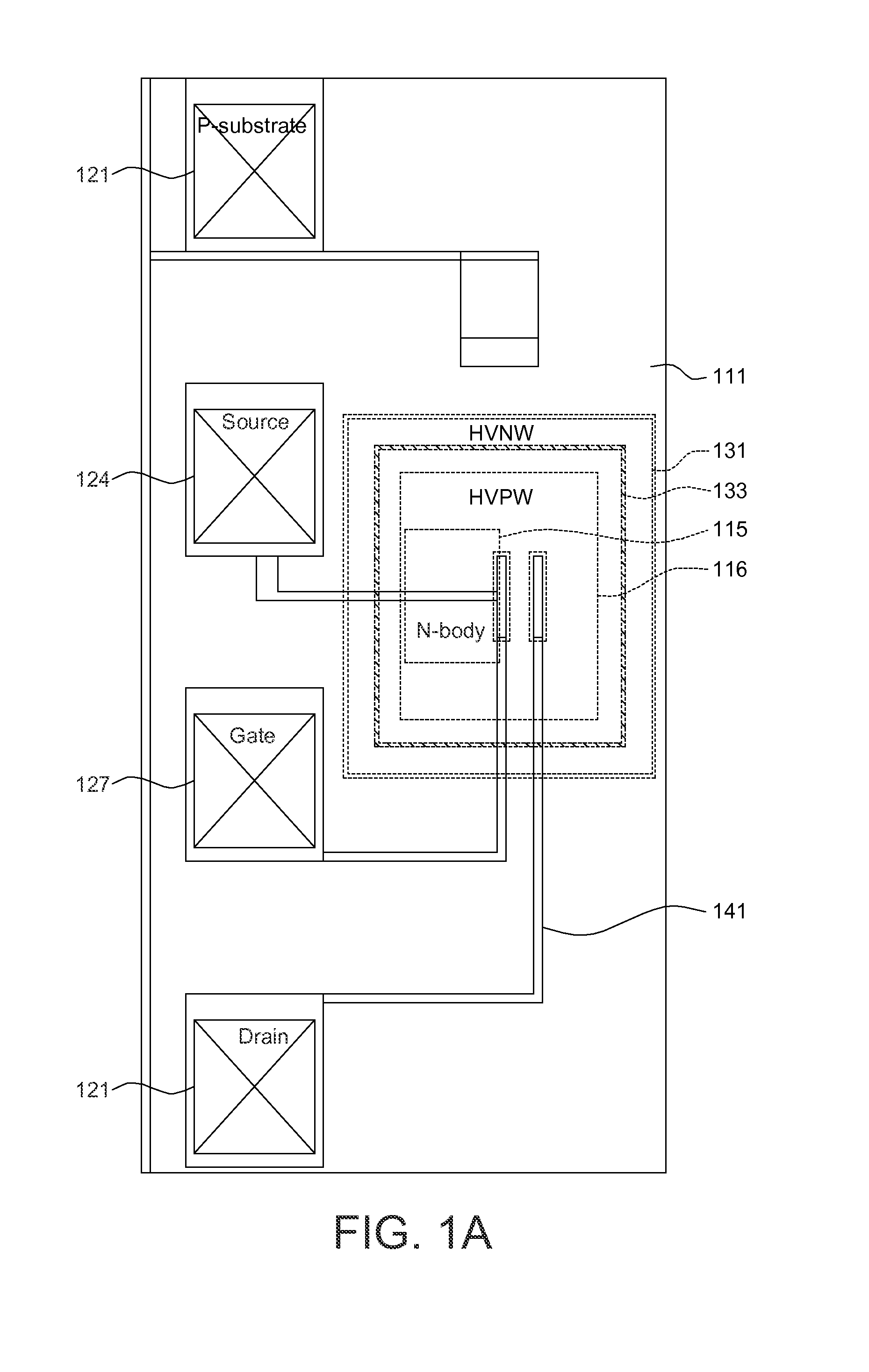
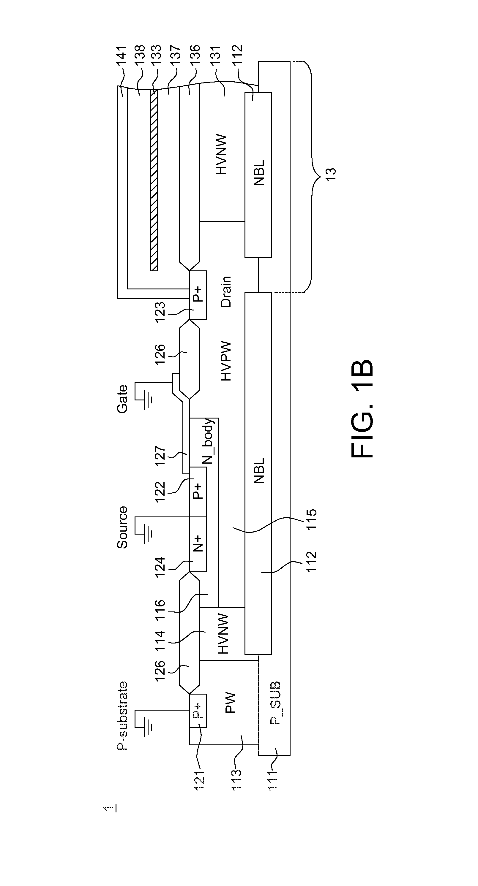
[0023]In one embodiment, the conductive body 133 could be a conductive ring surrounding the second well (e.g. the HVPW 115) and beneath the conductive line 141, as shown in FIG. 1A. However, the disclosure is not limited thereto. In practical applications, various shapes of the conductive body 133 could be adopted, such as circular, rectangular, elliptic shapes . . . etc, or a ring portion of those shapes, or other planes without interfering with other components, for achieving effect of voltage difference distribution and effectively improving the threshold voltage (Vth) of the field device. In the first embodiment, when the HVMOS 1 is under high voltage operation and a high voltage is applied to the conductive line 141, configuration of the field device 13 effectively avoids the field device turned on by applying no external voltage to the conductive body 133.

[0024]In the above description of the embodiment, P-type and N-type are exemplified as the first and second conductive type...

second embodiment

[0026]In the field device 23 of the second embodiment, the conductive body 233 is disposed under the conductive line 141, and further electrically connected to an external voltage source for applying a fixed voltage bias to the conductive body 233. Fabrication of the conductive body 233 could also be adopted in the current manufacturing process, and no extra cost and device area are required.

[0027]In the second embodiment, the conductive body 233 could be floating metal or conductive ring with a fixed voltage bias. When the HV semiconductor device is under high voltage operation, measurement results have indicated that the conductive body 233 pattern floating or fixed voltage biases (e.g. Metal 1=0V / −10V) can avoid the field device 23 turned on. In one example, when −150V is applied to the conductive line 141, the conductive body 233 could be applied with 0V, −10V, −20V, −30V, −40V, −70V, −80V . . . or other fixed voltage bias value. It is noted that the fixed voltage bias value is ...

third embodiment

[0029]In the third embodiment, the conductive body 333 of the field device 33 is disposed between the first well (e.g. HVNW 131) and the conductive line 141, and the field device 33 further comprises a second doping region 332 formed in the first well (e.g. HVNW 131) for interrupting continuity of the first well. The second doping region 332 and the first well have the same dosage type (e.g. the second conductive type), and the doping concentration of the second doping region 332 is larger than the doping concentration of the first well, and the second doping region 332 is electrically connected to the conductive body 333. In one embodiment, the second doping region 332 is a heavily doped region. The second doping region 332 with high doping concentration keeps isolation of the first well (e.g. HVNW 131) workable.

[0030]As shown in FIG. 3, the conductive body 333 comprises a body portion 333a and a pillar portion 333b connected to the body portion 333a, and the pillar portion 333b ex...


PUM


Abstract

A field device and method of operating high voltage semiconductor device applied with the same are provided. The field device includes a first well having a second conductive type and second well having a first conductive type both formed in the substrate (having the first conductive type) and extending down from a surface of the substrate, the second well adjacent to one side of the first well and the substrate is at the other side of the first well; a first doping region having the first conductive type and formed in the second well, the first doping region spaced apart from the first well; a conductive line electrically connected to the first doping region and across the first well region; and a conductive body insulatively positioned between the conductive line and the first well, and the conductive body correspondingly across the first well region.

Description

BACKGROUND[0001]1. Field of the Invention[0002]The disclosure relates in general to a field device and method of operating high voltage (HV) semiconductor device applied with the same, and more particularly to a field device which effectively improves turned on threshold voltage (Vth) of parasitic field device of the HV semiconductor device.[0003]2. Description of the Related Art[0004]There is currently an ongoing drive toward the downscaling of device dimensions in virtually all aspects of electronic device manufacture. Smaller electronic devices tend to be more popular than larger, more bulky devices when both devices have substantially equivalent capabilities. For high voltage (HV) or Ultra high voltage (UHV) semiconductor device (such as metal-oxide-semiconductor (MOS) devices), metal lines for connecting devices in silicon processes will induce parasitic field transistor turned on when metal lines pass through specific regions. It means that when MOSFETs is under high voltage o...

Claims


Application Information

Patent Timeline
Patent Type & Authority Patents(United States)
IPC IPC(8): H01L29/02H03K3/01H01L29/66
CPCH01L29/1095H01L29/1083H01L29/0696H01L29/1087H01L29/7816H01L29/402H01L29/404H03K17/16H03K17/56
Inventor CHENG, AN-LICHUNG, MIAO-CHUNHSU, CHIH-CHIAHUANG, YIN-FU
Owner MACRONIX INT CO LTD
Learn More