
Phase locked loop and method for operating the same

a phase lock and loop technology, applied in the direction of phase difference detection, pulse automatic control, angle demodulation, etc., can solve the problems of low power consumption, large external components of the plug-in, and low bandwidth of the plug-in, so as to achieve low power consumption, less external components, and low bandwidth

Active Publication Date: 2014-12-02
TEXAS INSTR INC
View PDF6 Cites 1 Cited by
  • Summary
  • Abstract
  • Description
  • Claims
  • Application Information

AI Technical Summary

Benefits of technology

[0005]It is another general object of the invention to provide a low-bandwidth PLL that can be built on a relatively small die. It is another general object of the invention to provide a PLL that requires less external components and consumes less power than PLLs according to the prior art. A further general object of the invention is to provide a low-bandwidth PLL that has lower peaking. Another object of the invention is to provide a better process compensation for a PLL.
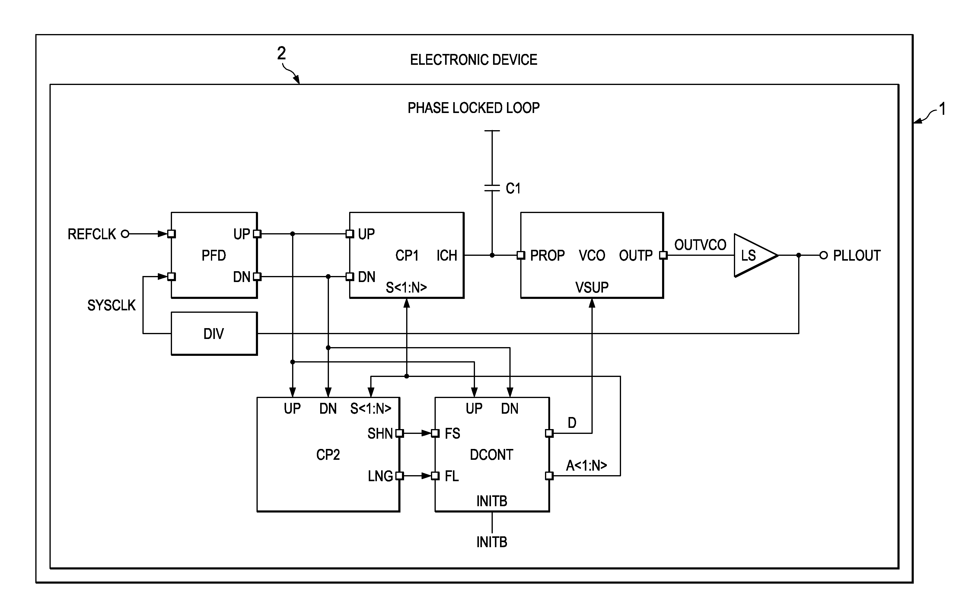
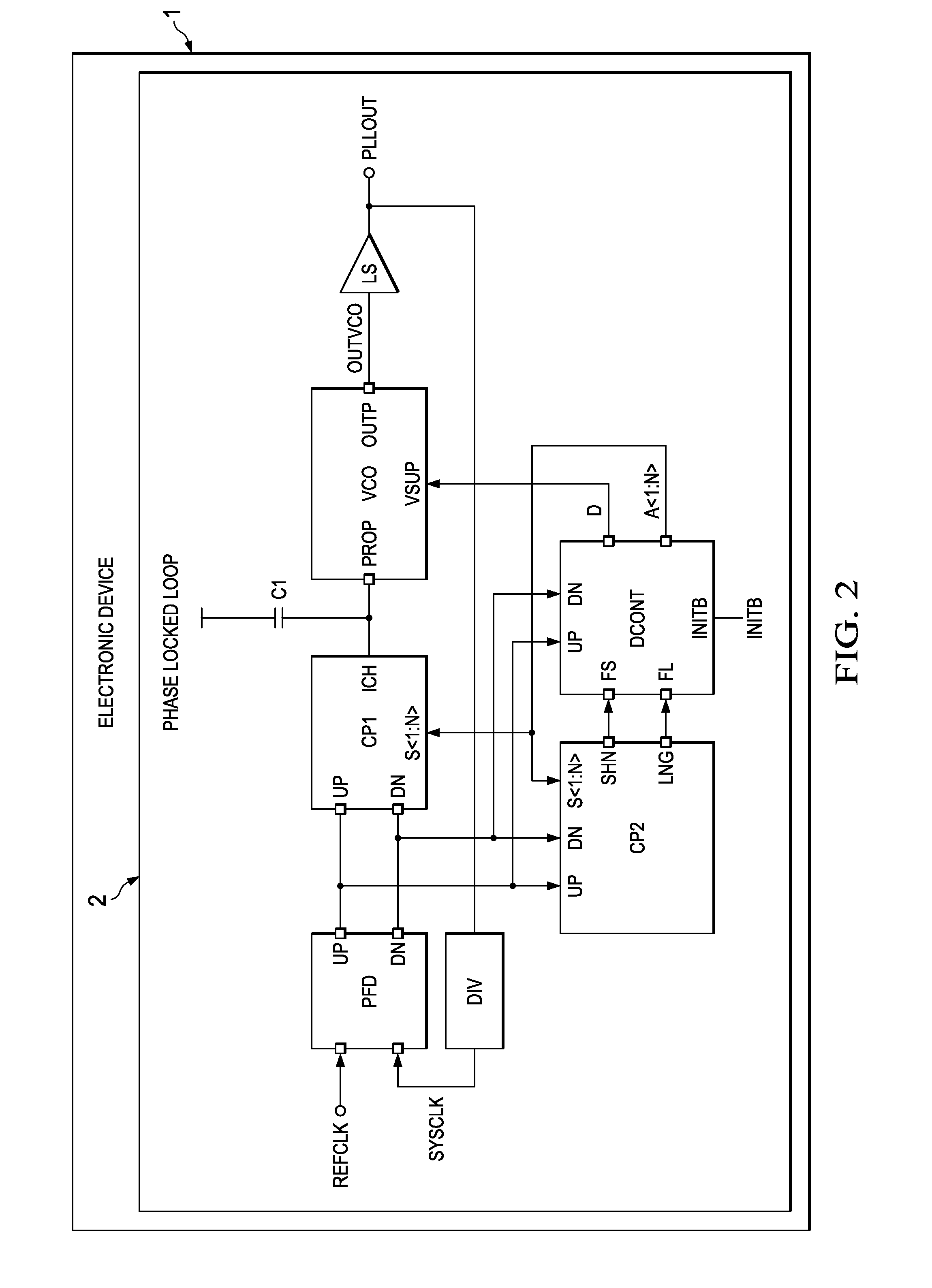
[0006]In a first aspect of the invention, a PLL is provided with a control stage that uses only two storage cells, a counter and a digital-to-analog (DAC) converter. In comparison to a PLL as for example described in European patent application EP 11 183 369.5 or published German patent application DE 10 2010 048 584 this configuration of the PLL's control stage reduces the chip area required for the PLL further, since the number of capacitors as well as the number of storage cells can be reduced. In example implementations using only two storage cells (and two storage capacitances), and in comparison to the example described in European patent application EP 11 183 369.5, where the storage cells share four capacitances, the reduction of the components in the control stage of the PLL may account for a reduction of 20% in the overall chip area.
[0008]A further, third aspect of the invention, which can be readily combined with the two before-mentioned aspects, allows implementing a PLL that has lower peaking in its frequency response, which results in better settling response. The frequency response peaking may be for example lowered by reducing the integral path gain of the PLL. In a semi digital architecture, as for example described in European patent application EP 11 183 369.5 or published German patent application DE 10 2010 048 584, or a PLL in line with the first aspect of the invention, this can be achieved by increasing the time to charge or discharge the storage cells' capacitors. To increase the storage cell charging / discharging time, either the charge pump current may be reduced or the storage cell capacitor size may be increased. In some applications, decreasing the charge pump current may not be desirable from a reliability perspective, since typically the charge pump current is already very low (e.g. in the one digit nA (nano Ampere) range, e.g. 1 nA). Increasing the area of the storage cells' capacitors will increase the area of the chip. Therefore, according to another exemplary implementation, it is proposed to sample the current through the integral path that charges the storage capacitor using a high speed clock signal, which may be for example in the GHz range (e.g. 1 GHz or higher). The duty cycle of the clock may be for example set to be less than 25% such that the storage capacitor is allowed to charge or discharge only 25% of the time. A duty ratio of 25% may decrease the effective charging current by a factor of 4, and may increase the charging time by the same amount, which can result in a reduced frequency peaking of the loop.
[0021]In one embodiment, the control signals are varied according to the output signal of the controlled oscillator or the control stage to thereby enable process-voltage-temperature compensation of the phase locked loop.

Problems solved by technology

PLLs with such low bandwidths require external components (such as large capacitors) and also consume a lot of power.
However, integrated circuits used in handheld and mobile devices require low power consumption and less number of external components while using as less chip area as possible.
In some applications, decreasing the charge pump current may not be desirable from a reliability perspective, since typically the charge pump current is already very low (e.g. in the one digit nA (nano Ampere) range, e.g. 1 nA).

Method used


Image

  • Phase locked loop and method for operating the same
  • Phase locked loop and method for operating the same
  • Phase locked loop and method for operating the same

Examples


Embodiment Construction

[0055]The invention generally relates to phase locked loops, and more specifically to low-bandwidth or ultra-low bandwidth phase locked loops. Low-bandwidth PLL may for example refer to a PLL having a bandwidth of 100 Hz to 1 kHz. An ultra-low bandwidth PLL may be for example a PLL having a lower bandwidth than a low-bandwidth PLL, which could be for example in the 1 Hz range or even lower. The invention may be for example embodied in an integrated circuit implementing a phase locked loop or in a circuit board, e.g. a printed circuit board providing a discrete implementation of the PLL. The invention could also be embodied in an electronic device or a method for operating a phase locked loop.

[0056]FIG. 2 shows an electronic device 1 including a PLL 2 in accordance with an exemplary embodiment of the invention. The PLL 2 includes a phase frequency detector PFD, an output of which is coupled to the input of the charge pump CP1. The output may include outputs UP and DN, on which phase ...


PUM


Abstract

The invention generally relates to phase locked loops (PLL), and more specifically to ultra-low bandwidth phase locked loops. The invention may be for example embodied in an integrated circuit implementing a phase locked loop or a method for operating a phase locked loop. The invention provides a PLL with a control stage that uses only two storage cells, a counter and a digital-to-analog (DAC) converter. In comparison to prior-art PLLs using storage cells the configuration of the invention's control stage reduces the chip area required for the PLL reduced. The invention further suggests PVT compensation mechanisms for a PLL and implementing a PLL that has lower peaking in its frequency response, which results in better settling response.

Description

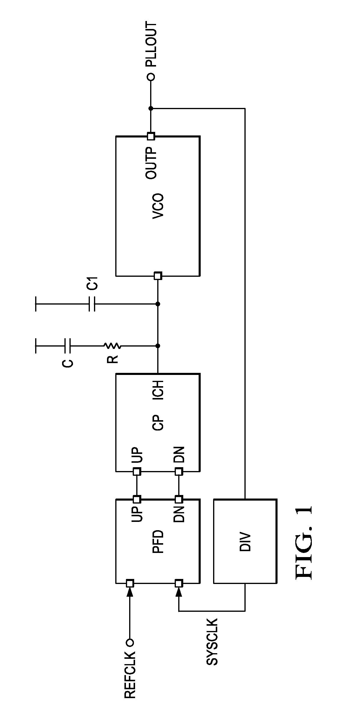
TECHNICAL FIELD[0001]The invention generally relates to phase locked loops (PLL), and more specifically to ultra-low bandwidth phase locked loops. The invention may be for example embodied in an integrated circuit implementing a phase locked loop or a method for operating a phase locked loop. The integrated circuit implementing the phase locked loop could be for example part of an electronic device.TECHNICAL BACKGROUND[0002]Phase locked loops are typically equipped with controlled oscillators, for example a voltage controlled oscillator (VCO). The VCO is coupled in a feedback loop in order to generate a high frequency clock from a low frequency reference clock. This reference clock is of a lower frequency since it is easier to generate various stable and precise clock signals at lower frequencies. An example of a phase locked loop according to the prior art is shown in FIG. 1. There is a VCO, a phase frequency detector PFD, a charge pump, a divider DIV and a compensation capacitor C...

Claims


Application Information

Patent Timeline
Patent Type & Authority Patents(United States)
IPC IPC(8): H03L7/089H03L7/06
CPCH03L7/0893H03L7/0995H03L1/00H03L7/0898H03L2207/06
Inventor SAREEN, PUNEETDIETL, MARKUSDEWAN, KETANGEORGE, EDMOND F.
Owner TEXAS INSTR INC
Learn More