Nitride based quantum well light-emitting devices having improved current injection efficiency

a quantum well and efficiency improvement technology, applied in the field of nitride-based quantum wells with current injection efficiency, can solve the problem of low efficiency achieved with typical gallium nitride-based quantum wells, and achieve the effect of reducing efficiency-droop and high internal quantum efficiency

Active Publication Date: 2014-12-09
LEHIGH UNIVERSITY
View PDF17 Cites 3 Cited by
  • Summary
  • Abstract
  • Description
  • Claims
  • Application Information

AI Technical Summary

Benefits of technology

[0012]The present invention provides a III-nitride based (e.g., GaN based) semiconductor device including a symmetrical arrangement of multi-layer barrier layers that provides improved internal quantum efficiency and reduced efficiency-droop by suppressing thermionic carrier escape from the quantum well active region, even at high (e.g., for J>200 A / cm2, and preferably up to J>650 A / cm2) current density. The symmetrical arrangement includes a quantum well active layer of a first nitride-based material having a relatively low bandgap characteristic (such as InGaN), and a pair of matched multi-layer barrier layers sandwiching the quantum well active layer. Each multi-layer barrier layer includes at least two layers of distinctly different materials—an inner layer abutting the quantum well active layer that is constructed of a relatively higher-bandgap material (such as AlInN or AlnGaN or AlGaN), and an outer layer of a relatively lower-bandgap material (such as GaN) having a higher bandgap than the bandgap of the quantum well active layer. In a preferred embodiment, the inner barrier layer is thinner than the outer barrier layer, and optionally, thinner also than the active layer.
[0013]Such a symmetrical arrangement of matched, multi-layer barrier layers immediately adjacent a quantum well active layer advantageously reduces carrier leakage from the quantum well active layer (e.g., InGaN) to an adjacent barrier region (e.g., GaN), even at high carrier density, which in turn leads to reduction of efficiency-droop.

Problems solved by technology

However, only low efficiency can be attained with typical gallium nitride-based quantum wells, such as InGaN-based quantum wells, particularly as emission wavelength is extended beyond green spectral regime and into the yellow and red spectral regimes.

Method used


Image

  • Nitride based quantum well light-emitting devices having improved current injection efficiency
  • Nitride based quantum well light-emitting devices having improved current injection efficiency
  • Nitride based quantum well light-emitting devices having improved current injection efficiency

Examples


Embodiment Construction

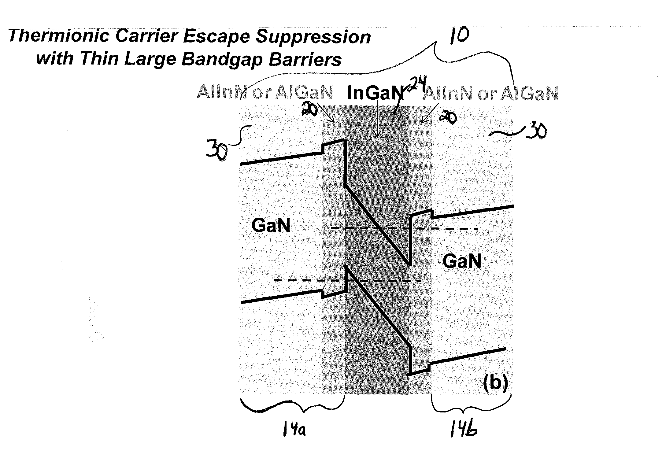
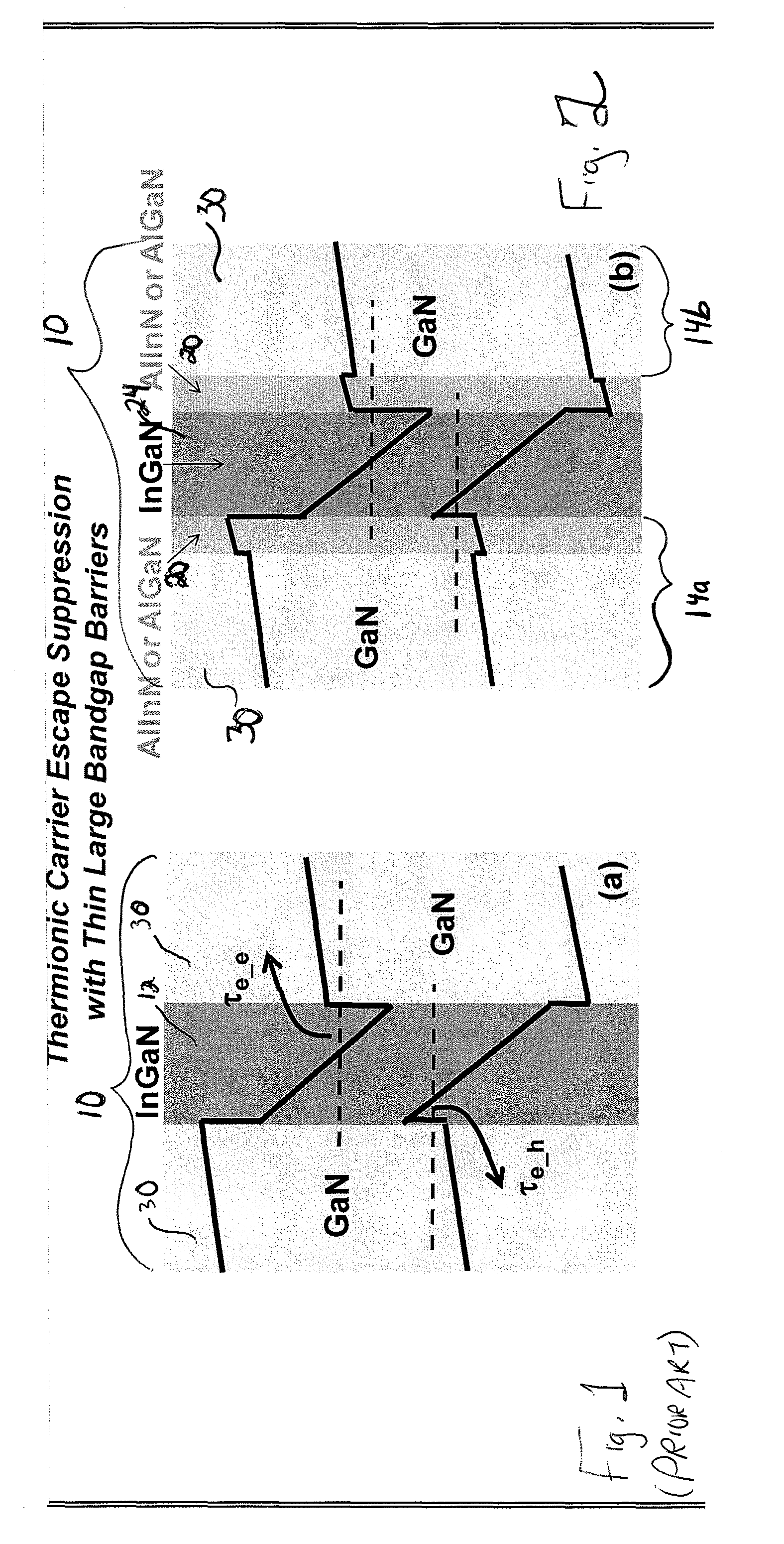
[0025]The present invention provides a III-Nitride based (e.g., GaN-based) semiconductor LED having an enhanced internal quantum efficiency that is achieved by adding a pair of layers of a large bandgap material between the quantum well active layer and the adjacent barrier layers of a conventional quantum well structure. Accordingly, the present invention provides a III-nitride based semiconductor device including a quantum well active layer and a pair of multi-layer barrier layers arranged symmetrically about the active layer. Each multi-layer barrier layer includes an inner layer abutting the quantum well active layer; and an outer layer abutting the inner layer. The inner barrier layer has an energy bandgap characteristic greater than that of the active layer. Further, the inner barrier layer has an energy bandgap characteristic greater than that of the outer barrier layer. The large bandgap inner barrier layers act as barriers to surround the central active layer and to suppres...


PUM


Abstract

A III-nitride based device provides improved current injection efficiency by reducing thermionic carrier escape at high current density. The device includes a quantum well active layer and a pair of multi-layer barrier layers arranged symmetrically about the active layer. Each multi-layer barrier layer includes an inner layer abutting the active layer; and an outer layer abutting the inner layer. The inner barrier layer has a bandgap greater than that of the outer barrier layer. Both the inner and the outer barrier layer have bandgaps greater than that of the active layer. InGaN may be employed in the active layer, AlInN, AlInGaN or AlGaN may be employed in the inner barrier layer, and GaN may be employed in the outer barrier layer. Preferably, the inner layer is thin relative to the other layers. In one embodiment the inner barrier and active layers are 15 Å and 24 Å thick, respectively.

Description

CROSS-REFERENCE TO RELATED APPLICATIONS[0001]This application claims the benefit of priority under 35 U.S.C. §119(e) of U.S. Provisional Patent Application No. 61 / 286,821, filed Dec. 16, 2009, the entire disclosure of which is hereby incorporated herein by reference.STATEMENT OF GOVERNMENT INTEREST[0002]This invention was made with government support under U.S. National Science Foundation—ECCS Award #0701421, and US Department of Energy—NETL (DE-FC26-08NT01581). The government has certain rights in the invention.FIELD OF THE INVENTION[0003]The present invention relates generally to semiconductor light-emitting devices (LEDs) including a III-nitride based a quantum well, and more particularly to a semiconductor LED having improved current injection efficiency (reduced efficiency-droop).DISCUSSION OF RELATED ART[0004]A quantum well is a potential boundary that confines particles to a planar, substantially two dimension region. As used herein, the term “quantum well” refers to a thin-l...

Claims


Application Information

Patent Timeline
Patent Type & Authority Patents(United States)
IPC IPC(8): H01L33/32H01L33/06H01L29/06
CPCH01L33/32H01L33/06
Inventor TANSU, NELSONZHAO, HONGPINGLIU, GUANGYUARIF, RONALD
Owner LEHIGH UNIVERSITY
Why Eureka
Try Eureka