System and method of in-system repairs or configurations for memories

a technology of in-system repair and configuration, applied in the field of system and method of in-system repair or configuration of memories, can solve the problems of faulty memory in the system, time-consuming and costly installation of new chips/modules, and the removal of old parts from the system, so as to reduce the cost of users, time-consuming and costly

Active Publication Date: 2014-12-16
ATTOPSEMI TECH CO LTD
View PDF168 Cites 60 Cited by
  • Summary
  • Abstract
  • Description
  • Claims
  • Application Information

AI Technical Summary

Benefits of technology

[0010]Embodiments disclosed herein use various schemes to repair and / or configure a memory while already provided in a system. Faulty memory in a system can be due to fatigue, wear out, stress, degraded performance (e.g., due to aging) or opens / shorts. When a memory chip is found faulty, the memory chip can be repaired or configured while installed in a system. This capability can substantially reduce costs for users, because the difficulties of finding replacement parts, taking the old parts off the system, and install new chips / modules can be very time consuming and costly.
[0014]As a memory for in-system repairs and configurations, one embodiment can, for example, include at least one OTP memory integrated into a memory chip or an SoC. The OTP memory can be programmed to store defective addresses and enable / disable bits, once an in-system repair or configuration mechanism is activated. The data programmed into the OTP memory can be read and verified. The program voltages can be supplied from the core and I / O voltages without additional high voltage supplies or additional pins for the memory chips. It is useful that the memory chips have the same pin outs and voltage supplies as memory chips without this capability. It is even more useful that the program voltages being less than 4.0V, or 3.3V in other embodiment, to prevent damaging the memory chips. After programmed, the data stored in the OTP memory can be used to compare with the incoming address in a match circuit to turn on the normal or redundant cells during memory accesses. To reduce the OTP cell size and the OTP program voltage, the OTP cell can be an electrical fuse cell using at least one diode in standard CMOS processes as program selector.
[0018]As a method for providing in-system repair or configuration mechanism for a memory, one embodiment can, for example, include at least one One-Time Programmable (OTP) memory in at least one memory chip and at least one repair program. When the system is found not functional, at least one diagnosis program can be run to determine if any memory chips have defects. If any of the memory chips are found having new defects or performance degraded and repairable, a program can be run to repair the defects by instructing a CPU or embedded processor to inform a memory controller to generate proper timing waveforms to program the defective addresses and enable / disable bits into the OTP memory. The data programmed into the OTP memory can be read and verified. The repair program can be downloaded from the Internet in real time and in-situ in another embodiment. The program voltages can be supplied from a core and I / O voltages without additional high voltage supplies or pins for the memory chips. It is useful for the memory chips the same pin outs and voltage supplies as memory chips without this capability. It is even more useful that the program voltage being less than 4.0V, or even 3.3V in other embodiment, to prevent damaging the memory chips. After programmed, the data stored in the OTP memory can be used to compare with an incoming address in a match circuit to select the normal or redundant cells, respectively, during memory access. To reduce the OTP cell size and the OTP program voltage, the OTP cell can be an electrical fuse cell using at least one diode in standard CMOS processes as program selector.

Problems solved by technology

Faulty memory in a system can be due to fatigue, wear out, stress, degraded performance (e.g., due to aging) or opens / shorts.
This capability can substantially reduce costs for users, because the difficulties of finding replacement parts, taking the old parts off the system, and install new chips / modules can be very time consuming and costly.

Method used


Image

  • System and method of in-system repairs or configurations for memories
  • System and method of in-system repairs or configurations for memories
  • System and method of in-system repairs or configurations for memories

Examples


Embodiment Construction

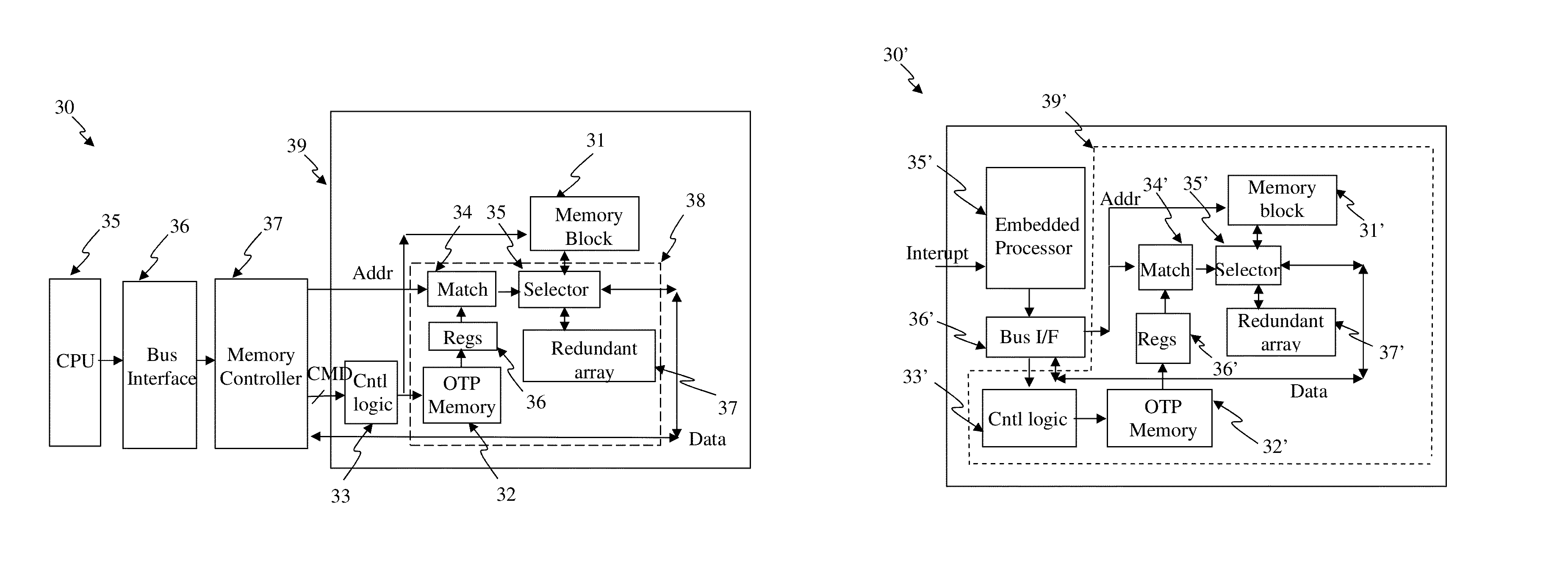
[0055]Embodiments disclosed herein use various schemes to repair and / or configure a memory while already provided in a system. Faulty memory in a system can be due to fatigue, wear out, stress, degraded performance (e.g., due to aging) or opens / shorts. When a memory chip is found faulty, the memory chip can be repaired or configured while installed in a system. This capability can substantially reduce costs for users, because the difficulties of finding replacement parts, taking the old parts off the system, and install new chips / modules can be very time consuming and costly.

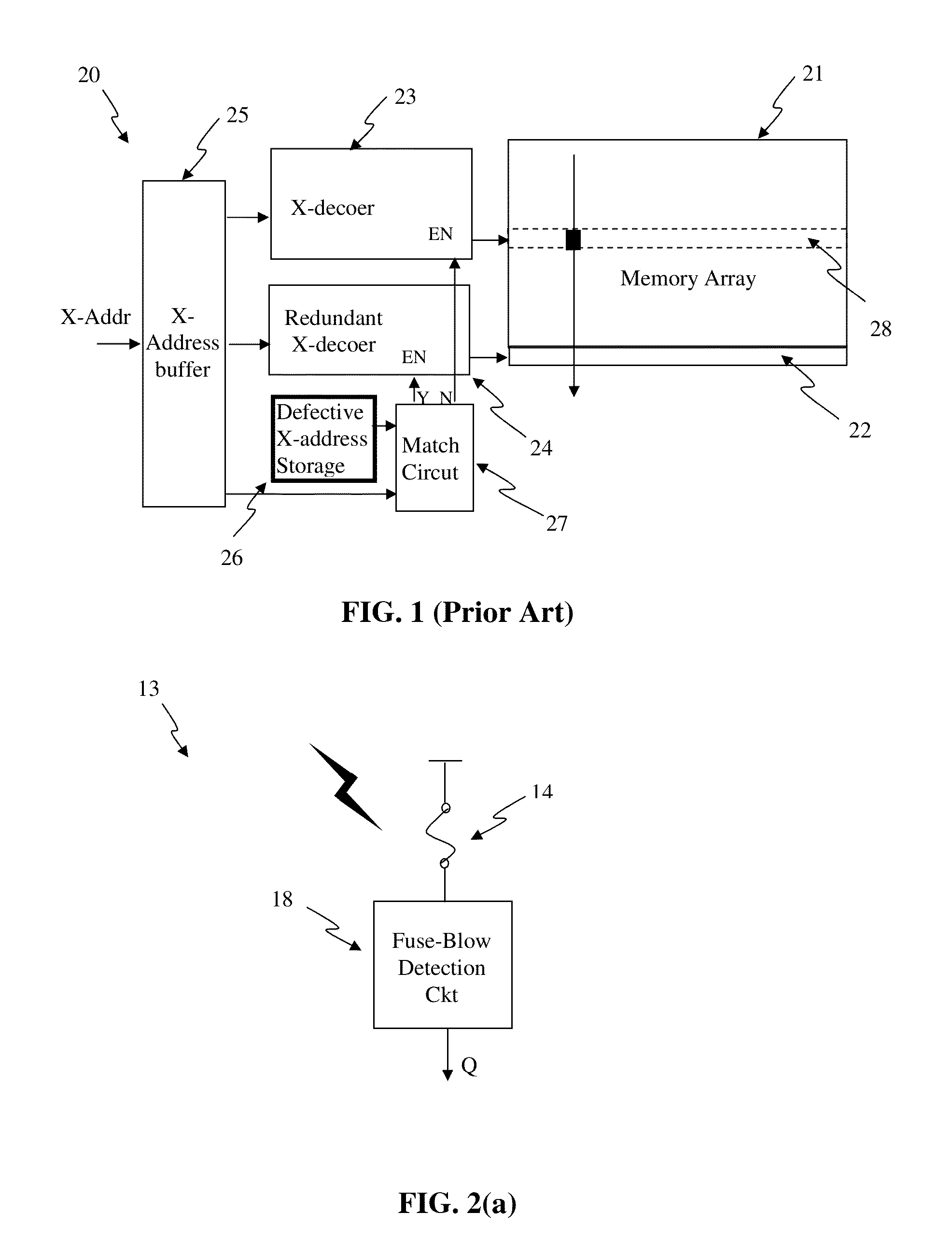
[0056]Semiconductor devices may degrade after being used in a system for long period of time. The device degradations can cause a high leakage current, a shift in threshold voltage, reduction in drain current, change to contact / via resistance, or degradation of gate-oxide integrity, etc. At a functional level, a semiconductor chip may become faulty because of device degradation. Particularly, a memory chip may h...


PUM


Abstract

In-system repairing or configuring faulty memories after being used in a system. In one embodiment, a memory chip can include at least one OTP memory to store defective addresses that are to be repaired. The OTP memory can operate without requiring additional I / O pins or high voltage supplies for reading or programming. The memory chip can also include control logic to control reading or programming of the OTP memory as needed.

Description

CROSS-REFERENCE TO RELATED APPLICATIONS[0001]This application claims priority benefit of: (i) U.S. Provisional Patent Application No. 61 / 668,031, filed on Jul. 5, 2012 and entitled “Circuit and System of Using Junction Diode as Program Selector and MOS as Read Selector for One-Time Programmable Devices,” which is hereby incorporated herein by reference; and (ii) U.S. Provisional Patent Application No. 61 / 609,353, filed on Mar. 11, 2012 and entitled “Circuit and System of Using Junction Diode as Program Selector for One-Time Programmable Devices,” which is hereby incorporated herein by reference.BACKGROUND OF THE INVENTION[0002]As memory capacity is becoming larger, a memory can have higher possibility of random defects, particle contaminations, or manufacturing inefficiencies such that the memory may not be useable. A conventional approach is to use spare cells to replace defective cells.[0003]FIG. 1 shows a block diagram of a portion of a conventional memory chip 20 as an example o...

Claims


Application Information

Patent Timeline
Patent Type & Authority Patents(United States)
IPC IPC(8): G11C29/00
CPCG11C17/18G11C17/16G11C17/12G11C17/00G11C29/785
Inventor CHUNG, SHINE, C.
Owner ATTOPSEMI TECH CO LTD
Why Eureka
Try Eureka