Touch screen and manufacturing method thereof

a technology of touch screen and manufacturing method, which is applied in the direction of electronic switching, pulse technique, instruments, etc., can solve the problem that it is difficult for the technology to form a fine pattern having high accuracy, and achieve the effect of ultrafine line width, excellent performance and high precision

Active Publication Date: 2014-12-30
LG CHEM LTD
View PDF69 Cites 1 Cited by
  • Summary
  • Abstract
  • Description
  • Claims
  • Application Information

AI Technical Summary

Benefits of technology

[0016]According to exemplary embodiments of the present invention, since a touch screen can comprise a conductive pattern with high precision and an ultrafine line width, the touch screen is excellent in performance and very efficient and economic in manufacturing method thereof. Further, the conductive pattern is in high precision and has the ultrafine line width and in addition, can have a large area.

Problems solved by technology

In order to solve the problem, a technology for displacing the ITO by using a printing method has been developed in a lot of corporations, but the technology is difficult to form a fine pattern having high accuracy which is invisible to the naked eye with respect to visibility.

Method used


Image

  • Touch screen and manufacturing method thereof
  • Touch screen and manufacturing method thereof
  • Touch screen and manufacturing method thereof

Examples


example 1

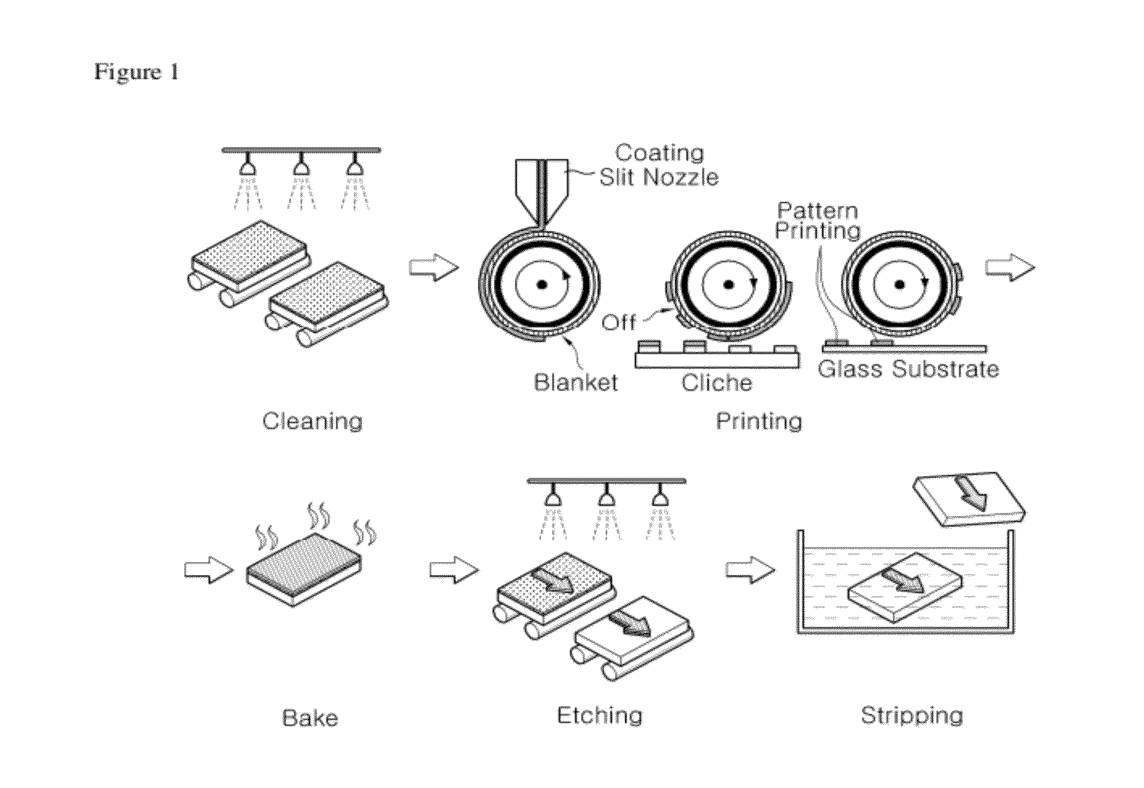
[0161]In order to manufacture a touch screen, a glass substrate in which an MoTi alloy with a thickness of 30 nm was deposited on glass of 0.5 t, Cu with a thickness of 200 nm was deposited thereon again, and Mo with a thickness of 30 nm was deposited thereon by using a sputtering process was manufactured.

[0162]Thereafter, etching resist ink (novolak resin composition (Product No. LG412DF made by LG CHEMISTRY, LTD. in KOREA)) was printed by using Cliché having a Voronoi irregular pattern having a size of 8 microns in line width and 200 microns in pitch through reverse offset printing. Thereafter, after a printed sample was baked at 130° C. for 3 minutes, the baked sample was etched (just etching time 30 sec) at 40° C. for approximately 110 seconds by using Cu etchant (ELCE-100) which is being prepared by ENF (Korea). Subsequently, the etching resist ink of the Voronoi pattern was removed.

[0163]A conductive pattern manufactured thereby was shown in FIG. 41 and the line width of the c...

example 2

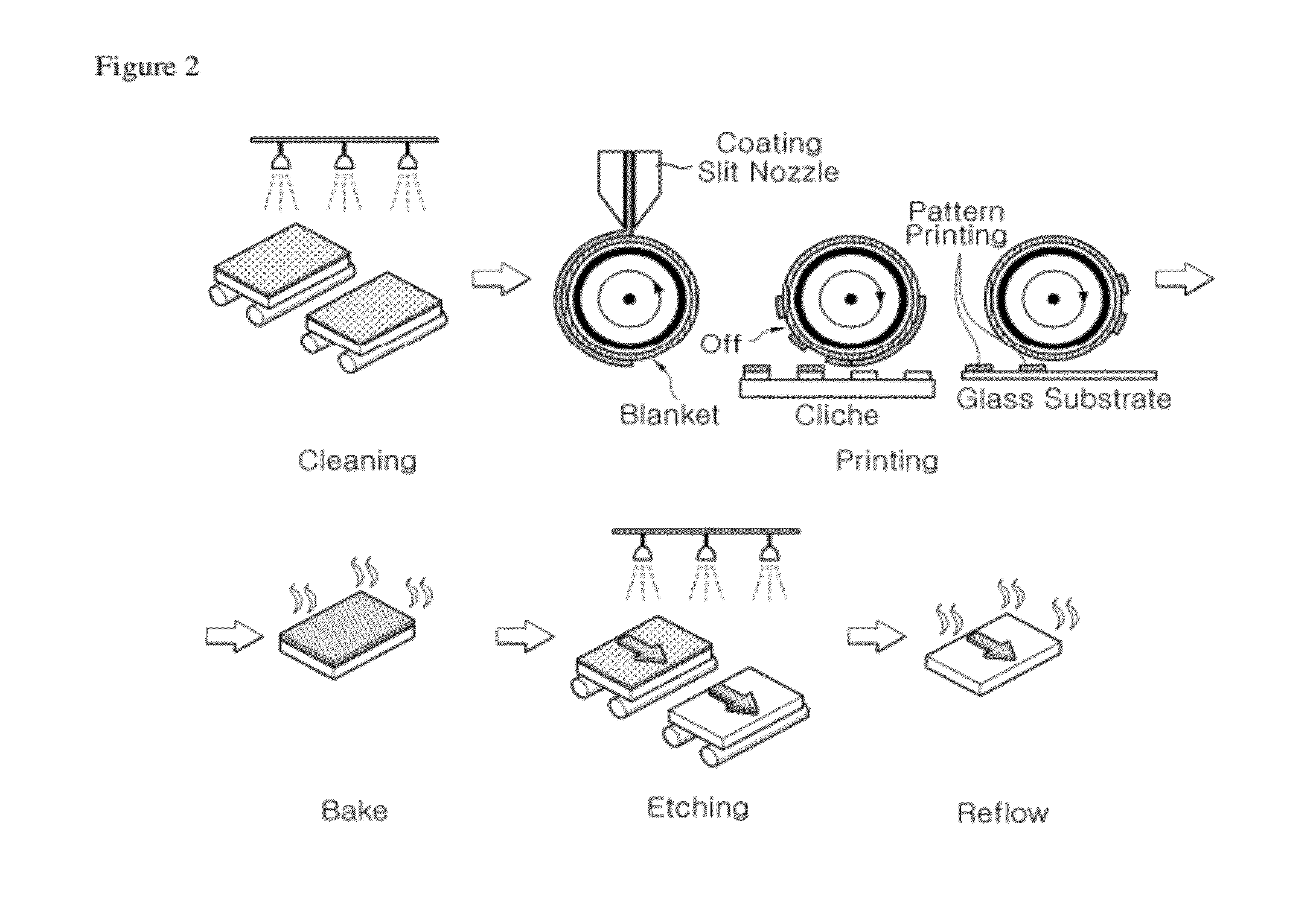
[0166]In order to manufacture a touch screen, a glass substrate in which an Ni metal with a thickness of 20 nm was deposited on glass of 0.5 t, Ag with a thickness of 200 nm was deposited thereon again, and Ni with a thickness of 20 nm was again deposited thereon by using the sputtering process was manufactured.

[0167]Thereafter, UV curable ink (LGP-7 made by NATOKO (Japan) was printed by using Cliché having the Voronoi irregular pattern having a size of 8 microns in line width and 200 microns in pitch through gravure offset printing.

[0168]Thereafter, after a printed sample was exposed through UV curing of approximately 500 mJ / cm2, the substrate was baked at 130° C. for 30 minutes. Subsequently, the baked substrate was etched (just etching time 20 sec) at 40° C. for approximately 60 seconds by using Al etchant (a mixed solution of phosphoric acid, nitric acid, acetic acid, and water) which is being prepared by ZEUS (Korea). A conductive pattern manufactured thereby was shown in FIG. ...


PUM

PropertyMeasurementUnit
widthaaaaaaaaaa
taper angleaaaaaaaaaa

Abstract

The present invention provides a method of manufacturing a touch screen, comprising the steps of: a) forming a conductive layer on a substrate; b) forming an etching resist pattern on the conductive layer; and c) forming a conductive pattern having a line width smaller than the line width of the etching resist pattern by over-etching the conductive layer by using the etching resist pattern and a touch screen manufactured by the method. According to the present invention, a touch screen comprising a conductive pattern having an ultrafine line width can be economically and efficiently provided.

Description

[0001]This application is a national stage application of PCT / KR / 2010 / 000762, filed Feb. 8, 2010, which claims priority from Korean Patent Application Nos. 10-2009-0009750, 10-2009-0065103, 10-2009-0065106, and 10-2009-0127756, filed on Feb. 6, 2009, Jul. 16, 2009, Jul. 16, 2009, and Dec. 21, 2009 in the Korean Intellectual Property Office, respectively, all of which are incorporated herein by reference in their entirety.TECHNICAL FIELD[0002]The present invention relates to a touch screen and a manufacturing method thereof.BACKGROUND ART[0003]In general, a touch screen is used by patterning an ITO-based conductive layer, but when the ITO is applied to a large-area touch screen, a recognition speed lowers due to self-RC relay. In order to solve the problem, a technology for displacing the ITO by using a printing method has been developed in a lot of corporations, but the technology is difficult to form a fine pattern having high accuracy which is invisible to the naked eye with respe...

Claims


Application Information

Patent Timeline
Patent Type & Authority Patents(United States)
IPC IPC(8): G06F3/044H03K17/975G06F3/041G06F3/045
CPCG06F3/044G06F3/041G06F2203/04112G06F3/045G06F2203/04103H05K3/4611H05K3/061G06F3/0445
Inventor HWANG, JI-YOUNGHWANG, IN-SEOKCHUN, SANG-KILEE, DONG-WOOKSON, YONG-KOOPARK, MIN-CHOONLEE, SEUNG-HEONKOO, BEOM-MOHONG, YOUNG-JUNKIM, KI-HWANKIM, SU-JINCHOI, HYEON
Owner LG CHEM LTD
Why Eureka
Try Eureka