Display device

a display device and display technology, applied in the field of display devices, can solve the problems of p-si-containing transistors, however, being prone to electrical characteristics variations

Inactive Publication Date: 2015-01-06
SEMICON ENERGY LAB CO LTD
View PDF11 Cites 14 Cited by
  • Summary
  • Abstract
  • Description
  • Claims
  • Application Information

AI Technical Summary

Problems solved by technology

Transistors containing p-Si, however, are prone to variations in electrical characteristics such as threshold voltage due to bonding defects at grain boundaries.

Method used


Image

  • Display device
  • Display device
  • Display device

Examples


embodiment 1

(Embodiment 1)

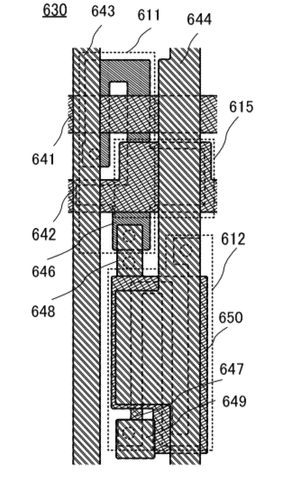
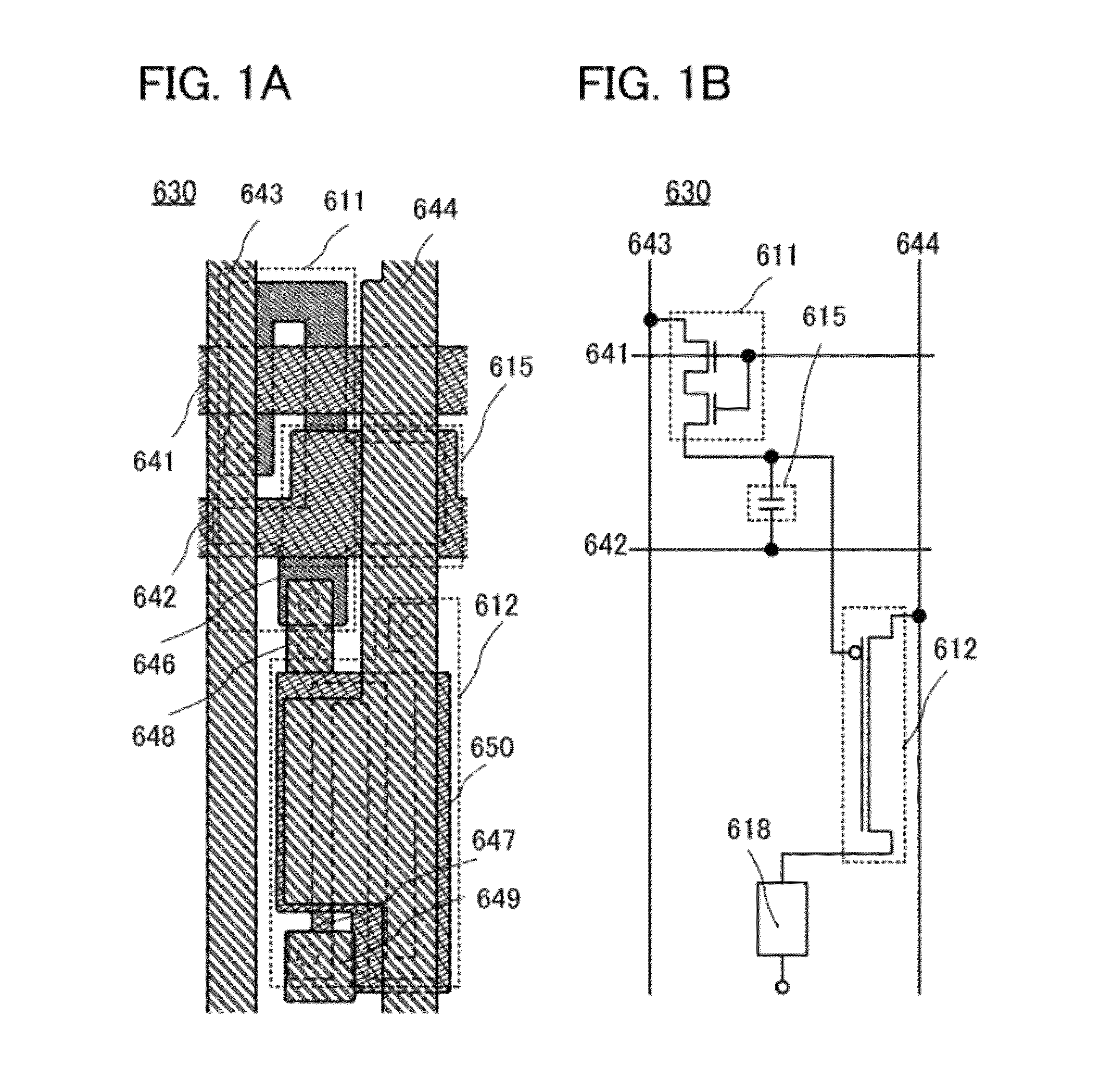
[0032]An active-matrix display device which is one embodiment of the present invention will be described with reference to FIGS. 1A and 1B and FIGS. 2A and 2B.

[0033]A light-emitting element (also called light-emitting display element) is used as a display element provided in a display panel included in the display device. Light-emitting elements include elements whose luminance is controlled by current or voltage, such as EL elements.

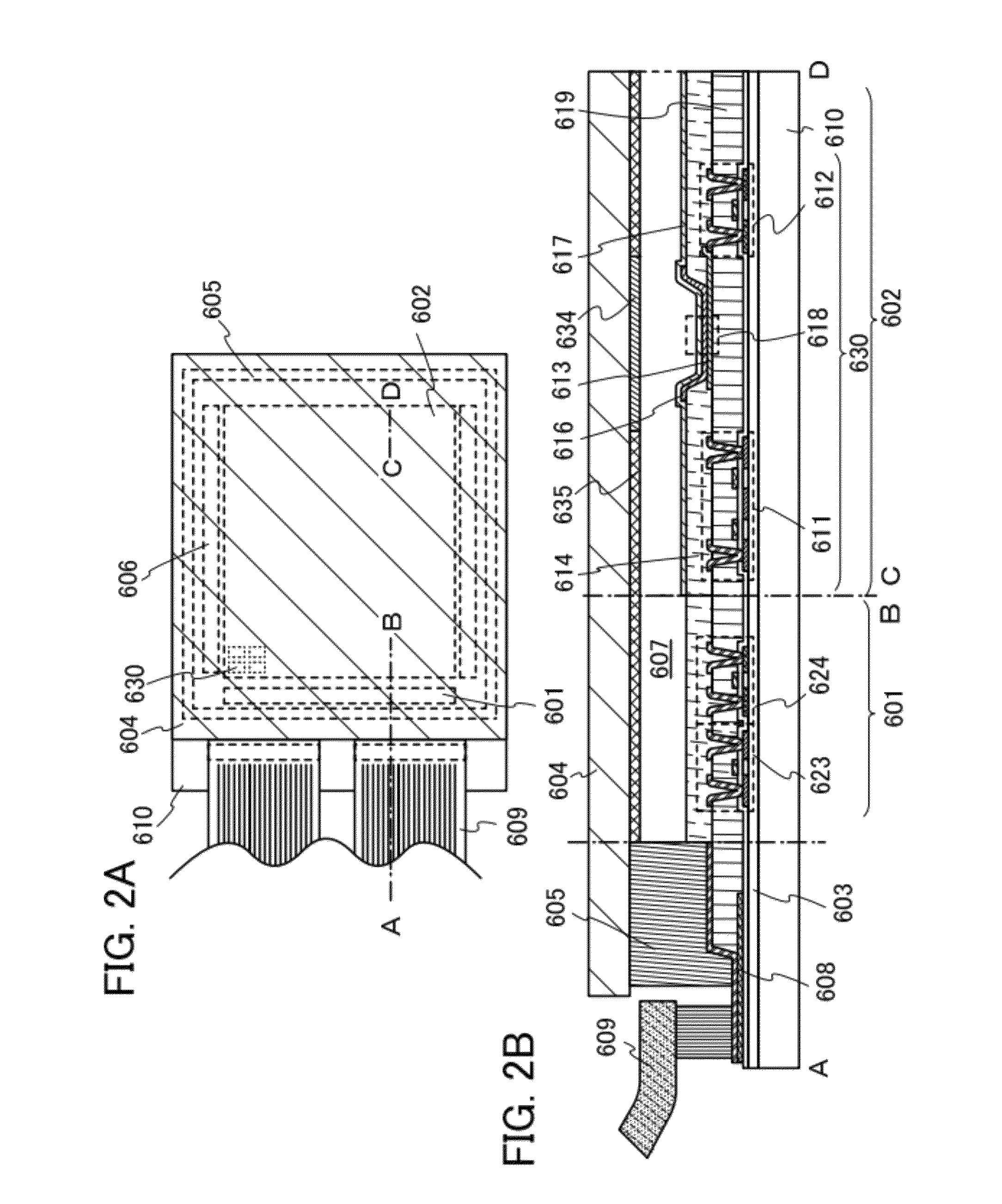
[0034]FIGS. 1A and 1B and FIGS. 2A and 2B show an example of the structure of a display device using an organic EL element as a display element. FIG. 2A is a plan view of a display device. FIG. 2B is a cross-sectional view along line A-B and C-D in FIG. 2A. An element substrate 610 adheres to a sealing substrate 604 by a sealant 605. The display device according to this embodiment includes a driver circuit area (a source driver circuit 601 and a gate driver circuit 606) and a pixel area 602 including a plurality of pixels 630.

[0035]Wiring ...

embodiment 2

(Embodiment 2)

[0084]In this embodiment, an example of an element structure of a light-emitting element exhibiting organic EL emission, which is used in a display device according to one embodiment of the present invention, will be described.

[0085]A light-emitting element shown in FIG. 3A includes the reflective electrode 613, the EL layer 616 over the reflective electrode 613, and the light-transmitting electrode 617 over the EL layer 616.

[0086]The EL layer 616 includes at least a light-emitting layer containing a light-emitting organic compound. In addition, the EL layer 616 can have a layered structure in which a layer containing a substance having a high electron transport property, a layer containing a substance having a high hole transport property, a layer containing a substance having a high electron injection property, a layer containing a substance having a high hole injection property, a layer containing a bipolar substance (a substance having a high electron transport pro...

embodiment 3

(Embodiment 3)

[0155]In this embodiment, display device that achieves three-dimensional (3D) image display and uses the display device according to the above embodiments as its display panel will be described with reference to drawings.

[0156]A display device shown in FIG. 4A includes a display panel 10 and a shutter panel 20. The display panel 10 includes a pixel area having a matrix of a plurality of pixels, specifically 350 pixels or more per one inch (i.e., the horizontal resolution is 350 ppi or more), more preferably 400 or more pixels per one inch (i.e., the horizontal resolution is 400 ppi or more); and a color filter layer overlapped with the pixel area. The shutter panel 20 is provided on the side where the display panel 10 emits light, that is, a side of the display device which is viewed by the viewer. Note that the display device shown in FIG. 4A uses the display device according to the above embodiments as the display panel 10.

[0157]The shutter panel 20 includes a plural...


PUM


Abstract

A display device includes a pixel area including pixels arranged in a matrix and having a horizontal resolution of 350 ppi or more and a color filter layer overlapping with the pixel area. The pixels each include a first transistor whose gate is electrically connected to a scan line and whose one of a source and a drain is electrically connected to a signal line; a second transistor whose gate is electrically connected to the other of the source and the drain of the first transistor and whose one of a source and a drain is electrically connected to a current-supplying line; and a light-emitting element electrically connected to the other of the source and the drain of the second transistor. The first and second transistors each have a channel formation region including a single crystal semiconductor.

Description

BACKGROUND OF THE INVENTION[0001]1. Field of the Invention[0002]One embodiment of the present invention relates to display devices, particularly to electroluminescent display devices. Another embodiment of the present invention relates to electronic devices including such display devices.[0003]2. Description of the Related Art[0004]Various electronic devices such as cellular phones and television receivers include display devices. Electroluminescent (EL) display devices using electroluminescent elements are attracting attention as display devices for their small thickness and light weight.[0005]An EL element in an EL display device is driven in accordance with the amount of the current flowing through the element. For this reason, each pixel in a display portion is connected to wiring for supplying current (current-supplying line). A current-supplying line is composed of a wire extended from outside a display region. Each pixel includes a transistor serving as a switching element fo...

Claims


Application Information

Patent Timeline
Patent Type & Authority Patents(United States)
IPC IPC(8): H01L33/08H01L51/50H01L27/112H01L27/12H01L27/32
CPCH01L27/3262H01L27/1225H01L27/1266H01L27/322H10K59/38H10K59/1213G09G3/30
Inventor YAMAZAKI, SHUNPEIIKEDA, TAKAYUKIAOKI, TAKESHIKOZUMA, MUNEHIRONAKAGAWA, TAKASHI
Owner SEMICON ENERGY LAB CO LTD
Why Eureka
Try Eureka