
Vertical cross point arrays for ultra high density memory applications

a memory array and vertical cross point technology, applied in the field of memory arrays, can solve the problems of diffraction limits, affecting the performance of memory cells in high-density memory arrays, and unable to scale down further, and achieve the effect of increasing capacity

Active Publication Date: 2015-01-20
UNITY SEMICON
View PDF131 Cites 66 Cited by
  • Summary
  • Abstract
  • Description
  • Claims
  • Application Information

AI Technical Summary

Benefits of technology

In this patent, the invention proposes a method to improve the efficiency and capacity of a vertical CMOS memory device. Instead of using bit line select devices that occupy area on the underlying substrate, the select devices are placed on top of the memory device, allowing for more logic circuitry and higher bit capacity without sacrificing memory cell density. This method also avoids the need for advanced lithography and shrink techniques. The technical effect of this invention is to improve the performance and capacity of vertical CMOS memory devices.

Problems solved by technology

However, the ability to scale down further is impeded by diffraction limits of the photolithography processes used in fabricating the floating gate transistors and by short channel effects and memory retention problems that arise when floating gate transistors are scaled down to nanometer dimensions.
However, various challenges to integrating the memory cells in high-density memory arrays remain.

Method used


Image

  • Vertical cross point arrays for ultra high density memory applications
  • Vertical cross point arrays for ultra high density memory applications
  • Vertical cross point arrays for ultra high density memory applications

Examples


Embodiment Construction

[0039]A detailed description of one or more examples is provided below along with accompanying figures. The detailed description is provided in connection with such examples, but is not limited to any particular example. The scope is limited only by the claims, and numerous alternatives, modifications, and equivalents are encompassed. Numerous specific details are set forth in the following description in order to provide a thorough understanding. These details are provided as examples and the described techniques may be practiced according to the claims without some or all of the accompanying details. For clarity, technical material that is known in the technical fields related to the examples has not been described in detail to avoid unnecessarily obscuring the description. The described fabrication techniques may be varied and are not limited to the examples provided.

[0040]Various embodiments or examples may be implemented in numerous ways, including as a system, a process, an ap...


PUM


Abstract

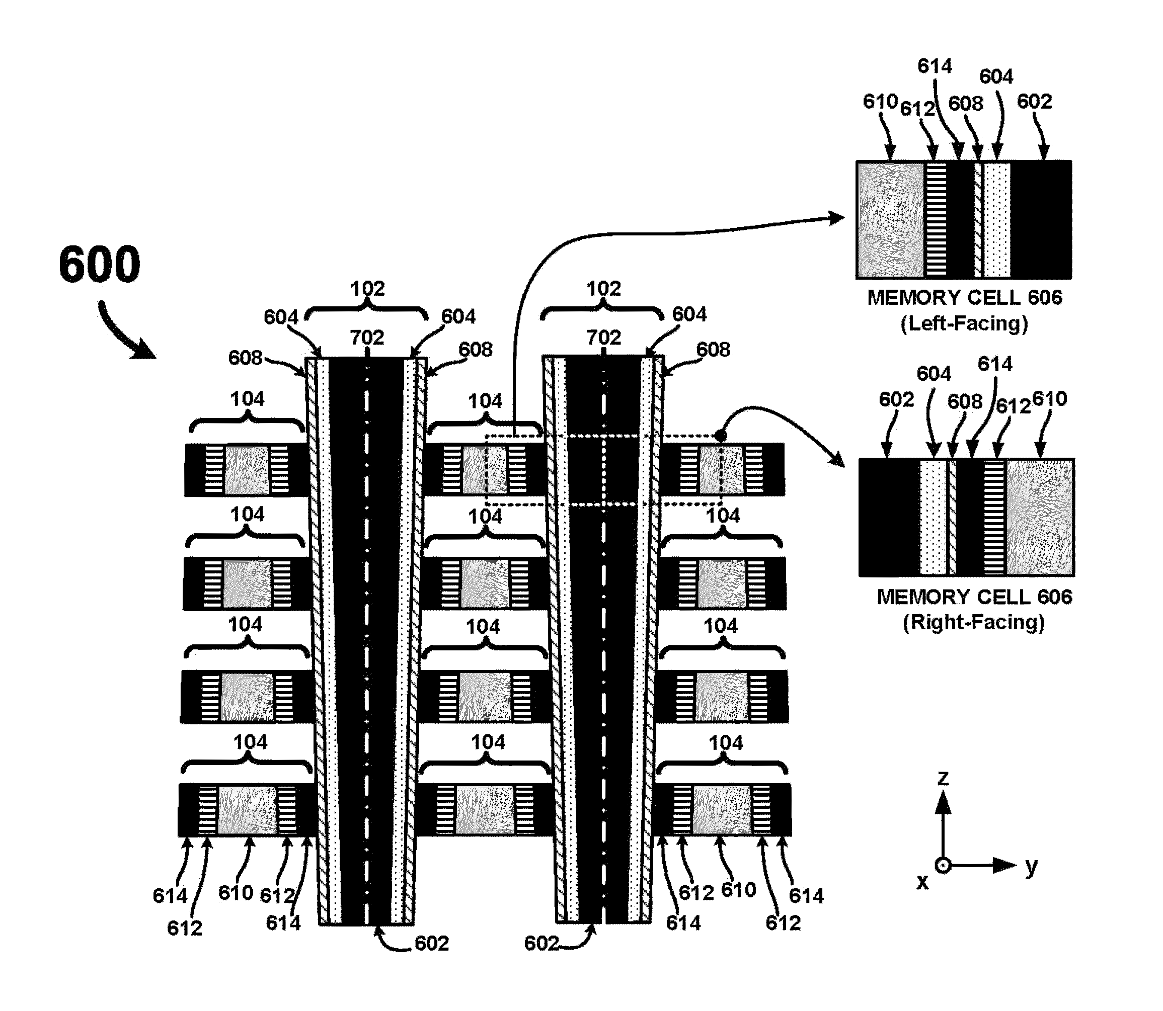
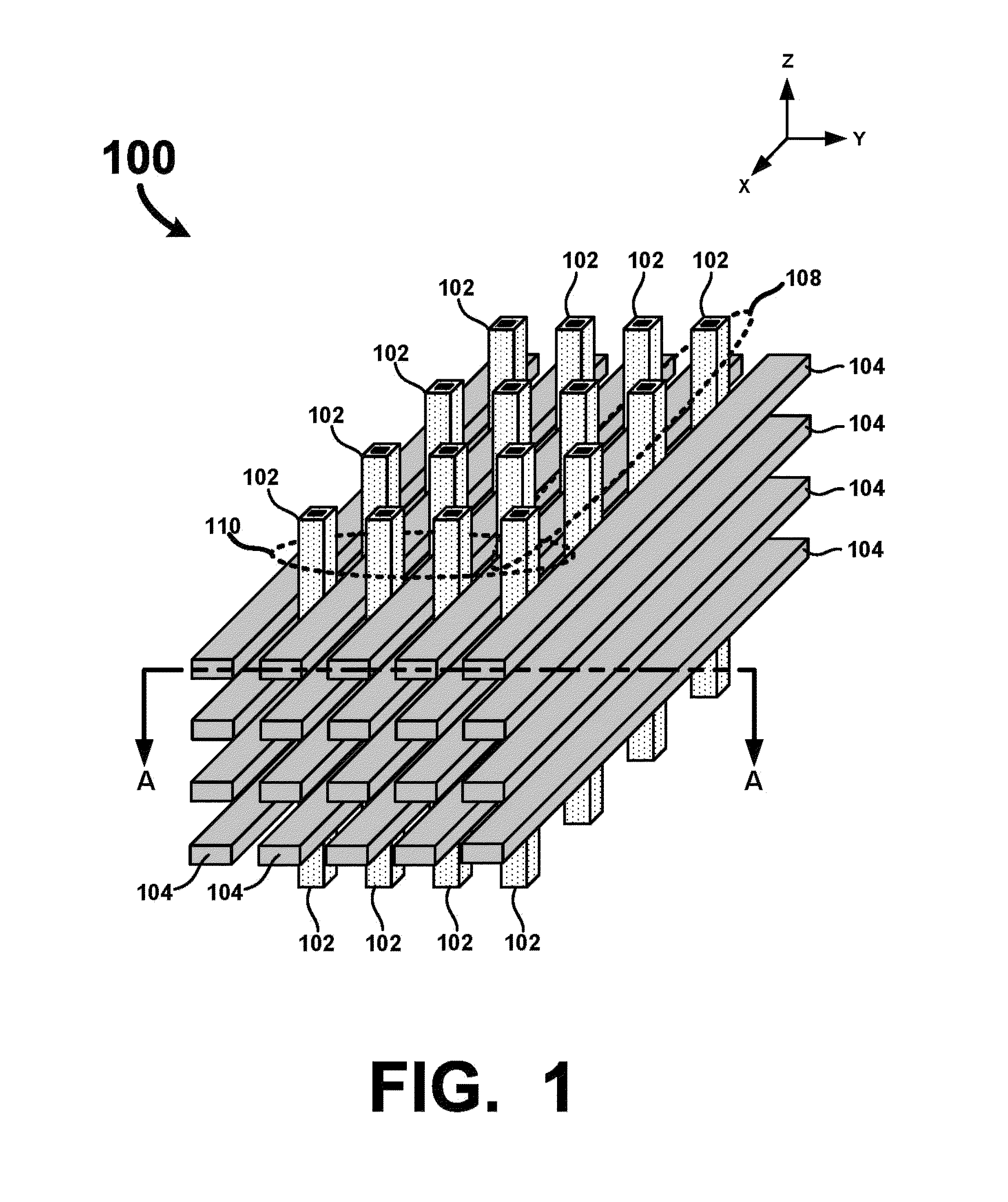
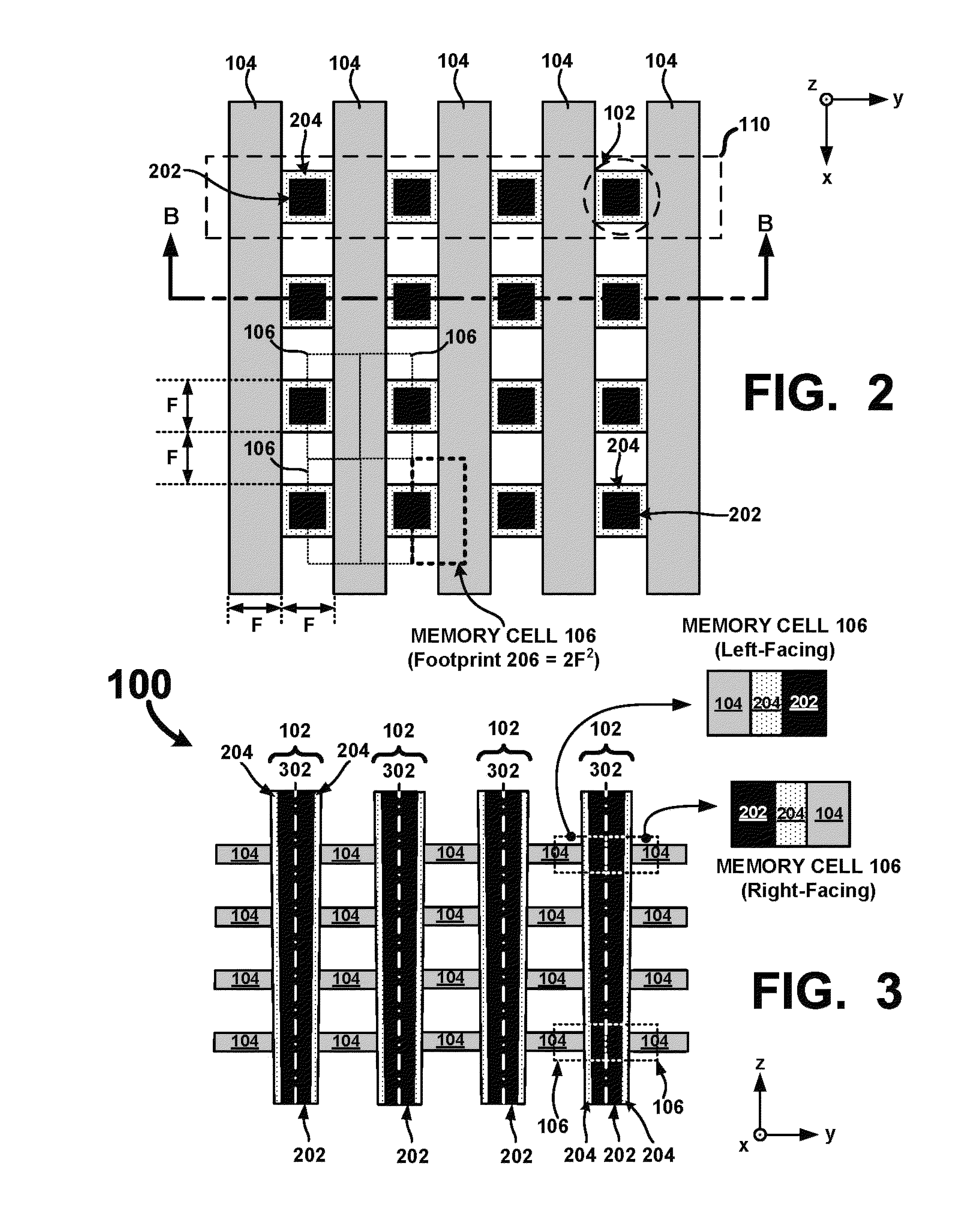
An ultra-high-density vertical cross-point array comprises a plurality of horizontal line layers having horizontal lines interleaved with a plurality of vertical lines arranged in rows and columns. The vertical lines are interleaved with the horizontal lines such that a row of vertical lines is positioned between each consecutive pair of horizontal lines in each horizontal line layer. Each vertical line comprises a center conductor surrounded by a single or multi-layered memory film. Accordingly, when interleaved with the horizontal lines, two-terminal memory cells are integrally formed between the center conductor of each vertical line and each crossing horizontal line. By configuring the vertical and horizontal lines so that a row of vertical lines is positioned between each consecutive pair of horizontal lines, a unit memory cell footprint of just 2F2 may be realized.

Description

FIELD OF THE INVENTION[0001]The present invention relates to memory arrays. More particularly, the present invention relates to back-end-of-the-line (BEOL) ultra-high-density vertical cross-point arrays (VCPAs) including two-terminal memory cells.BACKGROUND[0002]The availability of low-cost flash memory has been a major facilitator in the widespread proliferation of portable electronic devices such as smart phones, personal digital assistants, tablet and notebook computers, digital cameras, digital audio players, etc. It has also allowed the production of low-cost, flash-based solid-state drives (SSDs) which provide long-term persistent storage, similar to traditional hard disk drives (HDDs) but without the need for any moving parts. Flash memory is non-volatile, meaning that it retains its stored information even when not powered. It is also electrically erasable and reprogrammable, light-weight and durable, and requires no moving parts. All of these attributes lend well for use in...

Claims


Application Information

Patent Timeline
Patent Type & Authority Patents(United States)
IPC IPC(8): H01L27/24H01L45/00H10N70/10
CPCH01L27/2454H01L27/249H01L45/08H01L45/147H01L45/146H01L45/1226H10B63/34H10B63/845H10N70/24H10N70/823H10N70/8833H10N70/8836H10B63/22H10N70/826
Inventor BATEMAN, BRUCE
Owner UNITY SEMICON
Learn More