III-V finFETs on silicon substrate

a silicon substrate and finfet technology, applied in semiconductor devices, semiconductor/solid-state device details, electrical apparatus, etc., can solve the problem of not being able to employ a bottom-up approach for forming finfets on silicon substrates with iii-v materials

Active Publication Date: 2015-01-20
IBM CORP
View PDF12 Cites 41 Cited by
  • Summary
  • Abstract
  • Description
  • Claims
  • Application Information

AI Technical Summary

Problems solved by technology

However, no bottom-up approach is currently available that employs mass-production substrates with III-V materials for finFETs.

Method used


Image

  • III-V finFETs on silicon substrate
  • III-V finFETs on silicon substrate
  • III-V finFETs on silicon substrate

Examples


Embodiment Construction

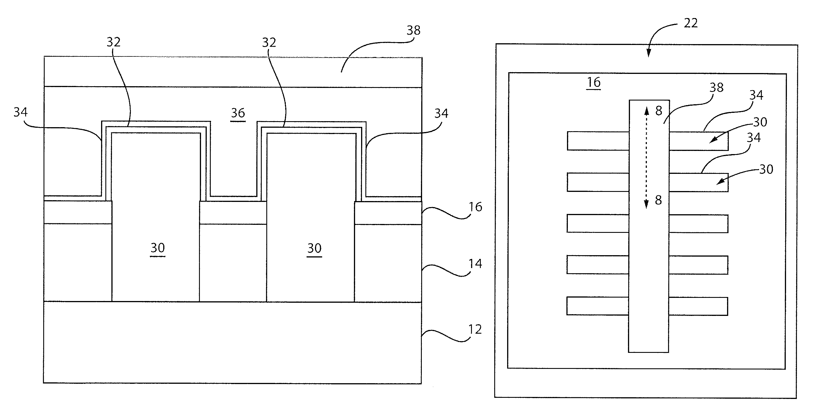
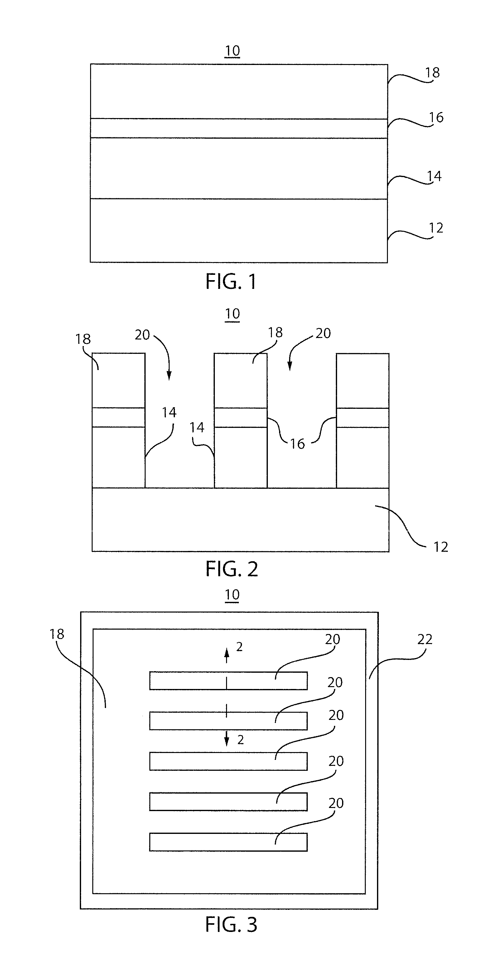
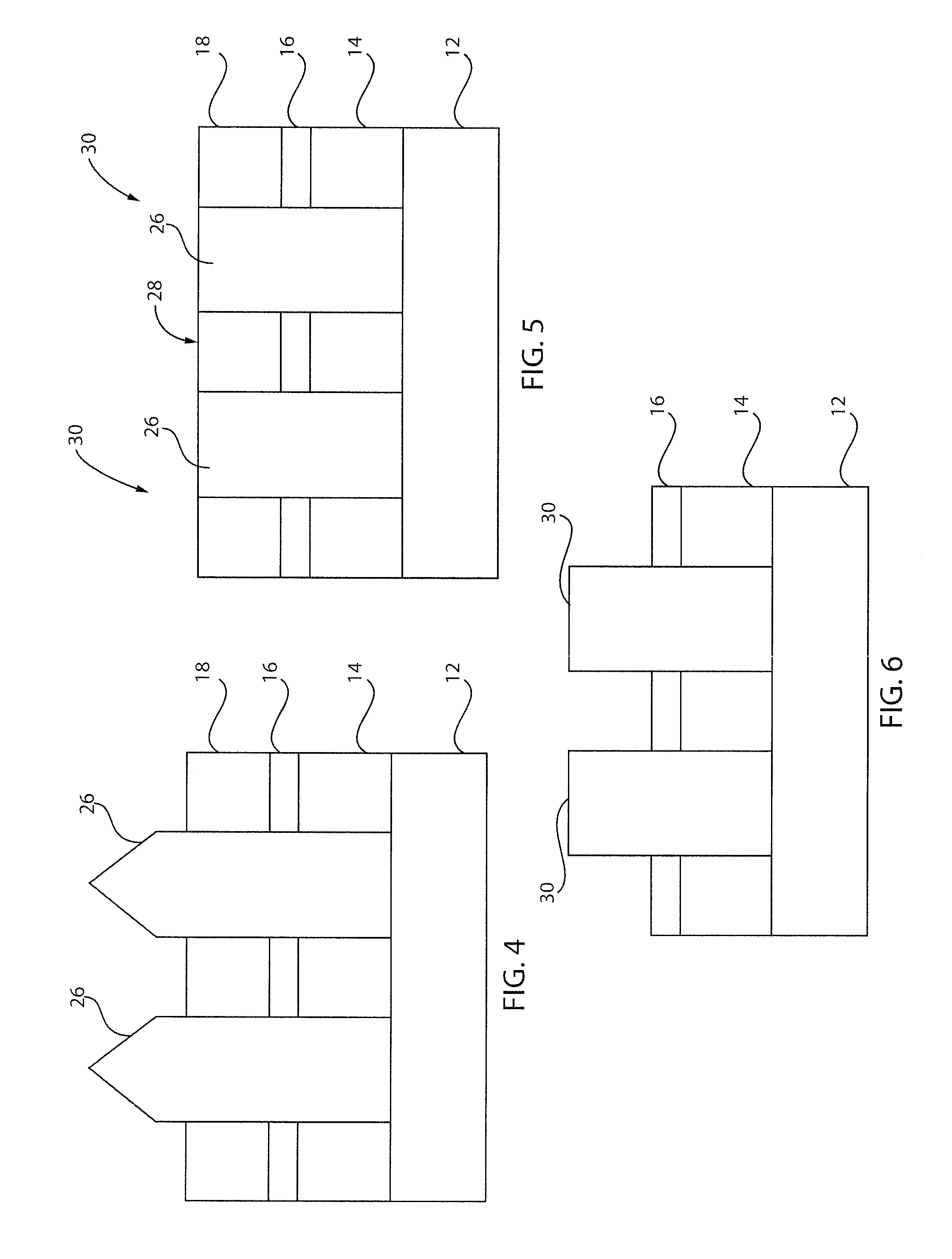
[0033]In accordance with the present principles, non-silicon material (e.g., III-V) fin field effect transistors (finFETs) are provided on silicon substrates. The present embodiments provide a number of variations for the finFET integration process. For example, while the present embodiments describe gate first, self-aligned, finFETs, the finFETs may also be formed using a gate last self-aligned, III-V finFET, a non-self-aligned, III-V finFET or these with other finFET materials. In addition, embodiments described herein may include implanted finFET extension regions or include fin chopping embodiments. In accordance with the present principles, silicon and non-silicon semiconductor materials can be combined on a same chip. For example, a III-V material, such as, indium phosphide and a group IV material, such as germanium can be integrated on a same device, which can provide structures for both the emission and detection of light, on silicon. In this way, manufacturers could combine...


PUM

PropertyMeasurementUnit
aspect ratioaaaaaaaaaa
thicknessaaaaaaaaaa
dielectric constantaaaaaaaaaa

Abstract

A method for forming fin field effect transistors includes forming a dielectric layer on a silicon substrate, forming high aspect ratio trenches in the dielectric layer down to the substrate, the high aspect ratio including a height to width ratio of greater than about 1:1 and epitaxially growing a non-silicon containing semiconductor material in the trenches using an aspect ratio trapping process to form fins. The one or more dielectric layers are etched to expose a portion of the fins. A barrier layer is epitaxially grown on the portion of the fins, and a gate stack is formed over the fins. A spacer is formed around the portion of the fins and the gate stack. Dopants are implanted into the portion of the fins. Source and drain regions are grown over the fins using a non-silicon containing semiconductor material.

Description

RELATED APPLICATION DATA[0001]This application is a Continuation application of co-pending U.S. patent application Ser. No. 13 / 800,398 filed on Mar. 13, 2013, incorporated herein by reference in its entirety.BACKGROUND[0002]1. Technical Field[0003]The present invention relates to semiconductor processing and devices, and more particularly to forming fin field effect transistors with III-V materials on silicon.[0004]2. Description of the Related Art[0005]Processing of silicon wafers is the most frequently employed type of wafer processing. The maturity and popularity of silicon wafer processing results in cost savings for its use, and only silicon substrates are suitable for mass manufacture due at least in part to their mechanical and electrical properties. However, many applications can benefit from mass-produced, higher-performance III-V materials.[0006]Fin field effect transistors (finFETs) are becoming more widely used for scaling down transistors on semiconductor devices. Howev...

Claims


Application Information

Patent Timeline
Patent Type & Authority Patents(United States)
IPC IPC(8): H01L29/78H01L29/267H01L29/49H01L29/51
CPCH01L29/66795H01L29/785
Inventor BASU, ANIRBANCHENG, CHENG-WEIMAJUMDAR, AMLANMARTIN, RYAN M.RANA, UZMASADANA, DEVENDRA K.SHIU, KUEN-TINGSUN, YANNING
Owner IBM CORP
Why Eureka
Try Eureka