Color-based linear three dimensional acquisition system and method

a three-dimensional acquisition and color-based technology, applied in the field of systems and methods for depositing materials, can solve the problems of limited scope of view of both area-scan and line-scan formats, and large imaging area may require substantial time, so as to reduce shadowing effects

Active Publication Date: 2015-01-27
ILLINOIS TOOL WORKS INC
View PDF22 Cites 10 Cited by
  • Summary
  • Abstract
  • Description
  • Claims
  • Application Information

AI Technical Summary

Benefits of technology

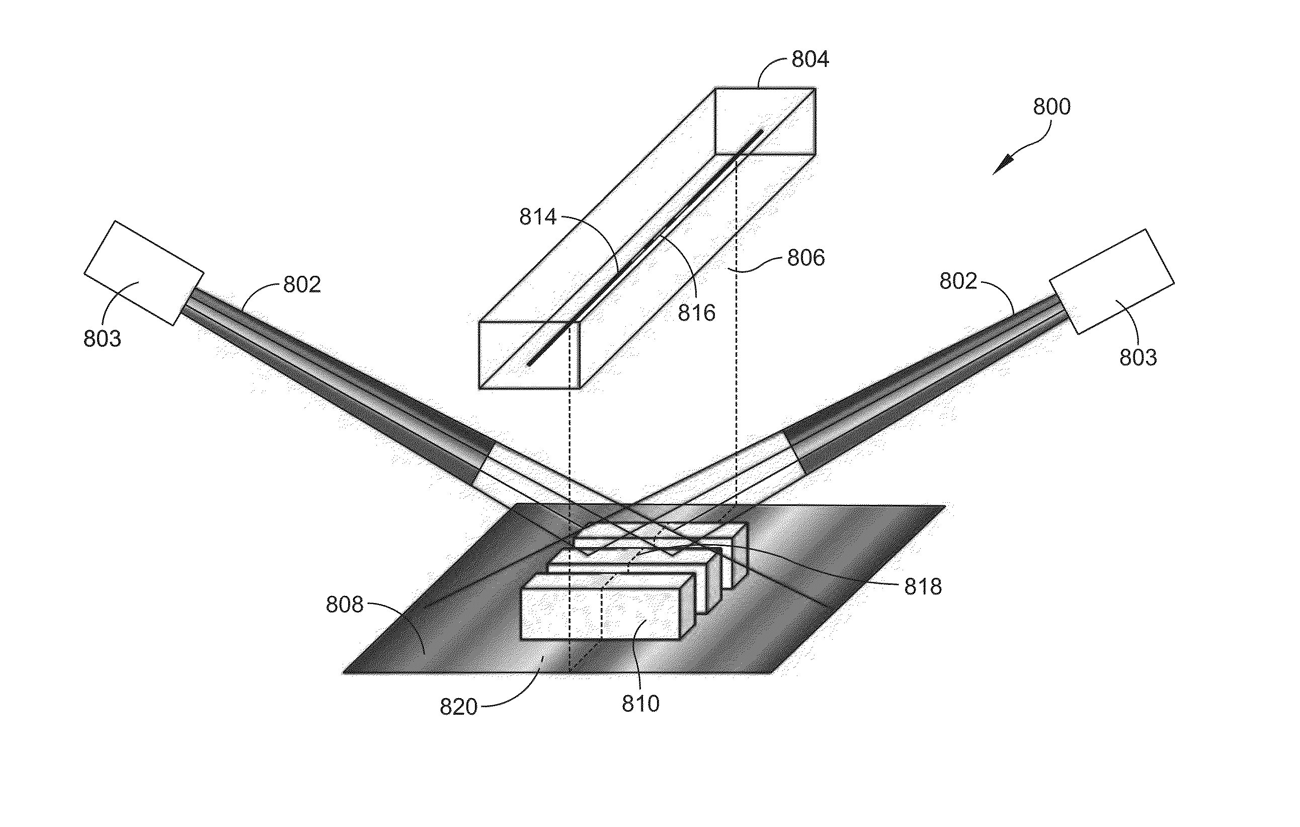
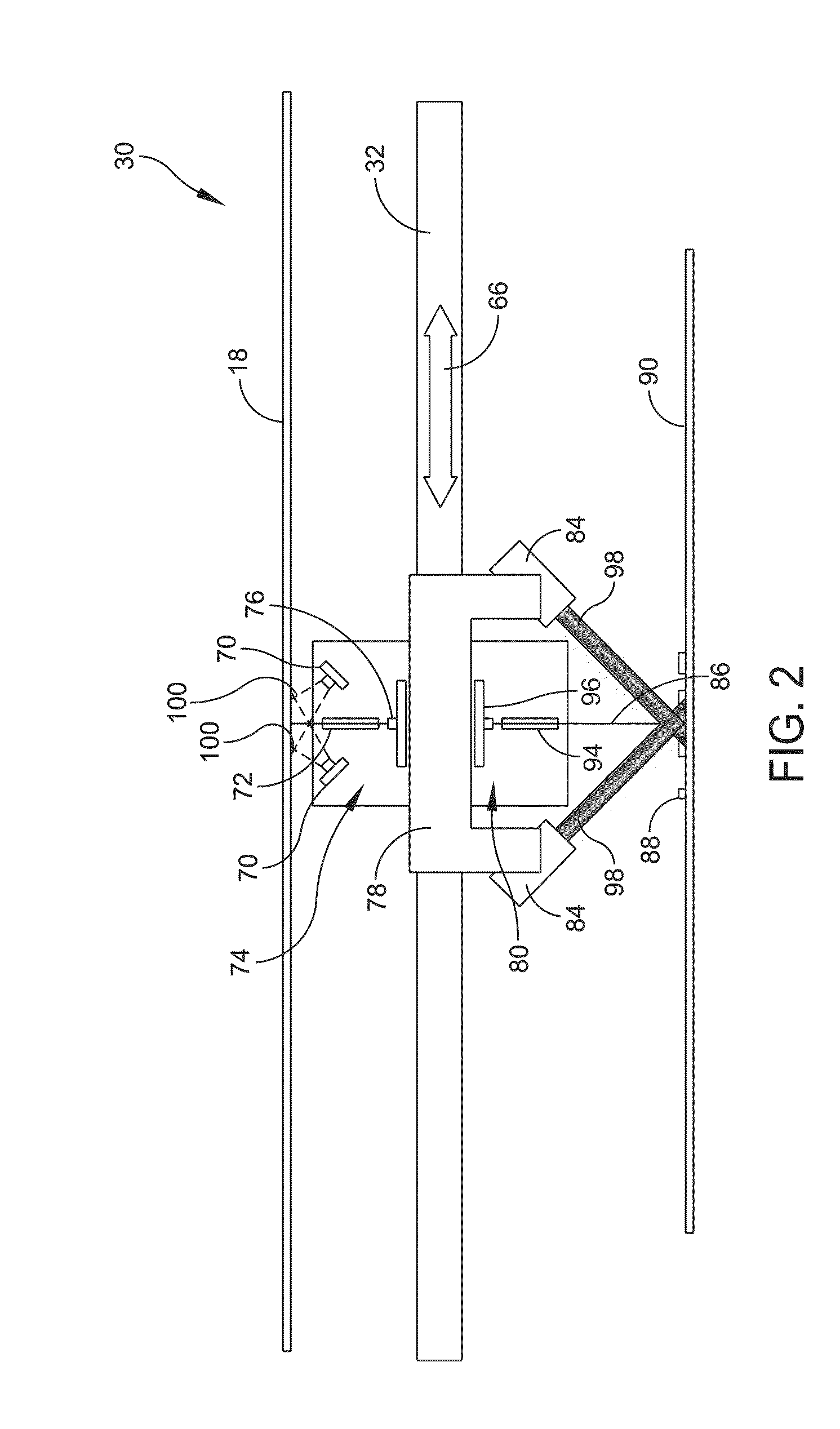
[0016]In accordance with another aspect, the method of imaging material on a substrate further comprises the acts of: positioning the electronic substrate in a print position; and positioning a stencil on the electronic substrate. In accordance with yet another aspect, the method of imaging material on a substrate further comprises the act of projecting the one or more spectrums of light in linear patterns. The projecting of one or more spectrums of light in linear patterns comprises projecting the linear patterns at opposing angles to strengthen measurable light where the linear patterns intersect along a viewing plane to reduce shadowing effects on the electronic substrate due to adjacent topologies, which, in certain embodiments the act includes aligning the linear patterns such that similar colors overlap over a range of elevations along the viewing plane. In accordance with yet another aspect, the method of imaging material on a substrate further comprises the act of moving the imaging system from a first position that captures three-dimensional image data of topology of a first area to a second position that captures three-dimensional image data of topology of a second area. According to another embodiment, the method of imaging material on a substrate further comprises splitting the spectrum of light into component colors, wherein, in certain embodiments, further comprising projecting a continuous spectrum of color.

Problems solved by technology

One challenge facing the design of such stencil printers and dispensing systems is the ability to perform a fast, comprehensive inspection of a large area of a substrate after the disposition of solder paste in a single pass.
Further, while methods have been developed to perform consistent two-dimensional modeling of solder paste on a substrate, e.g., the circuit board, through existing area-scan and line-scan formats, such approaches are limited various ways.
In typical practice, both area-scan and line-scan formats have a limited field of view as a result of the relatively short distance between the lens of the imaging system and the substrate.
For example, in area-scan format, imaging a large area may require substantial time as the imaging system moves point-to-point to acquire a large area of a substrate.

Method used


Image

  • Color-based linear three dimensional acquisition system and method
  • Color-based linear three dimensional acquisition system and method
  • Color-based linear three dimensional acquisition system and method

Examples


Embodiment Construction

[0031]For the purposes of illustration only, and not to limit the generality, the present disclosure will now be described in detail with reference to the accompanying figures. This disclosure is not limited in its application to the details of construction and the arrangement of components set forth in the following description or illustrated in the drawings. The principles set forth in this disclosure are capable of other embodiments and of being practiced or carried out in various ways. Also the phraseology and terminology used herein is for the purpose of description and should not be regarded as limiting. The use of “including,”“comprising,”“having,”“containing,”“involving,” and variations thereof herein, is meant to encompass the items listed thereafter and equivalents thereof as well as additional items.

[0032]Various embodiments of the present disclosure are directed to material deposition or application systems, devices including such material deposition systems, and methods...


PUM


Abstract

A system and method for capturing three-dimensional image data for inspection, alignment and operations of a material applicator includes an imaging system configured to capture three-dimensional image data of an electronic substrate. The imaging system includes one or more illumination assembly configured to project a spectrum of light substantially along a first axis at an angle to the surface of the electronic substrate. The imaging system further includes an image sensor assembly configured to detect the spectrum of light reflected from an electronic substrate surface, with the image sensor assembly including a viewing plane. The material application includes a controller that is coupled to the imaging system. The controller is configured to control movement of the imaging system and to communicate with the image sensor assembly to produce a three-dimensional image of the topology of the electronic substrate.

Description

BACKGROUND OF THE DISCLOSURE[0001]1. Field of the Disclosure[0002]This disclosure relates generally to systems and methods for depositing a material on a substrate, such as a printed circuit board, and more particularly to an apparatus and systems and methods for inspecting such deposits.[0003]2. Discussion of the Related Art[0004]There are several types of prior art material application systems used for depositing assembly materials, such as solder, for a variety of applications.[0005]One such application uses a stencil printer to print solder paste onto a circuit board. In a typical surface-mount circuit board manufacturing operation, a stencil printer is used to print solder paste or some other material onto the circuit board, which has a pattern of pads or some other conductive surface onto which solder paste will be deposited. The circuit board is automatically fed into the stencil printer and one or more small holes or marks on the circuit board, called fiducials, is used to p...

Claims


Application Information

Patent Timeline
Patent Type & Authority Patents(United States)
IPC IPC(8): B05C17/04B41L13/18G01B11/25H05K3/22H05K13/04H05K13/08
CPCH05K3/225G01B11/2509H05K13/0469H05K13/08G01N21/95684H05K13/0817
Inventor PRINCE, DAVID P.
Owner ILLINOIS TOOL WORKS INC
Why Eureka
Try Eureka