Method of producing a microacoustic component

a microacoustic component and microacoustic technology, applied in the direction of coatings, chemical vapor deposition coatings, special surfaces, etc., can solve the problems of uneconomical, process takes a long time, and the deposition rate is generally so low, and achieve the effect of excessive layer thickness fluctuations

Inactive Publication Date: 2015-01-27
SNAPTRACK
View PDF16 Cites 2 Cited by
  • Summary
  • Abstract
  • Description
  • Claims
  • Application Information

AI Technical Summary

Benefits of technology

[0010]In one aspect, the present invention specifies how the problem of excessively large layer thickness fluctuations can be eliminated in the case of microacoustic components.
[0012]In an atomic-layer-deposition method nearly any arbitrary metal or dielectric can be deposited by means of a precursor comprising an organic carrier. The deposition is done layer by layer such that atomic monolayers can be produced supported by reactive linking of the precursor to the surface to be covered by the ALD deposition. An arbitrary number of atomic monolayers can be deposited one above the other and a perfect control of the layer thickness is possible.
[0023]Generally, an ALD layer provides more advantages when more layers have to be deposited one above the other and more accuracy of the layer thickness is required. In a staple of layers, the bottom layer embodied as an ALD layer facilitates homogenous growth of the further layers above. A top layer embodied as an ALD layer allows deposition of a layer with a homogenous thickness on uneven surfaces.
[0025]Using ALD layers allows the enhancement of the number of layers that are to be deposited one above the other without diminishing quality and homogeneity of the layers. Preferably, ALD layers are used in components where component structures of two or more components are stacked directly above one another. Components comprising stacked SAW or BAW resonators can be manufactured with high quality and high yield.

Problems solved by technology

If dielectric layers are deposited by one of the methods mentioned, the deposition rate is generally so low that the process takes a very long time and can consequently become uneconomic if a large layer thickness of more than 1 μm is intended to be produced.
If thick metallizations are covered with a high metal proportion, cavities, so-called voids, can occur in the dielectric material, which significantly impair the properties of the component.
In the case of surface wave components provided with electrodes which are embodied in strip-type fashion and are intermeshed with one another in a comb-like manner, an undesirable material transport can occur, brought about by mechanical stress in the electrode material.
A sufficiently good coverage of the outer interfaces of the electrodes cannot always be achieved in the desired manner, however, with the deposition methods mentioned.
The adhesion of the layers produced by vapor deposition or sputtering in particular of hard layers, is inadequate under certain circumstances.

Method used


Image

  • Method of producing a microacoustic component
  • Method of producing a microacoustic component
  • Method of producing a microacoustic component

Examples


Embodiment Construction

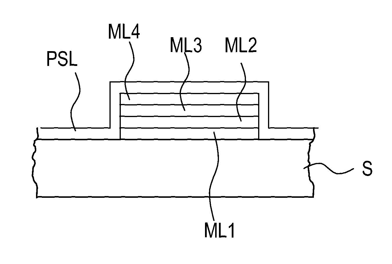
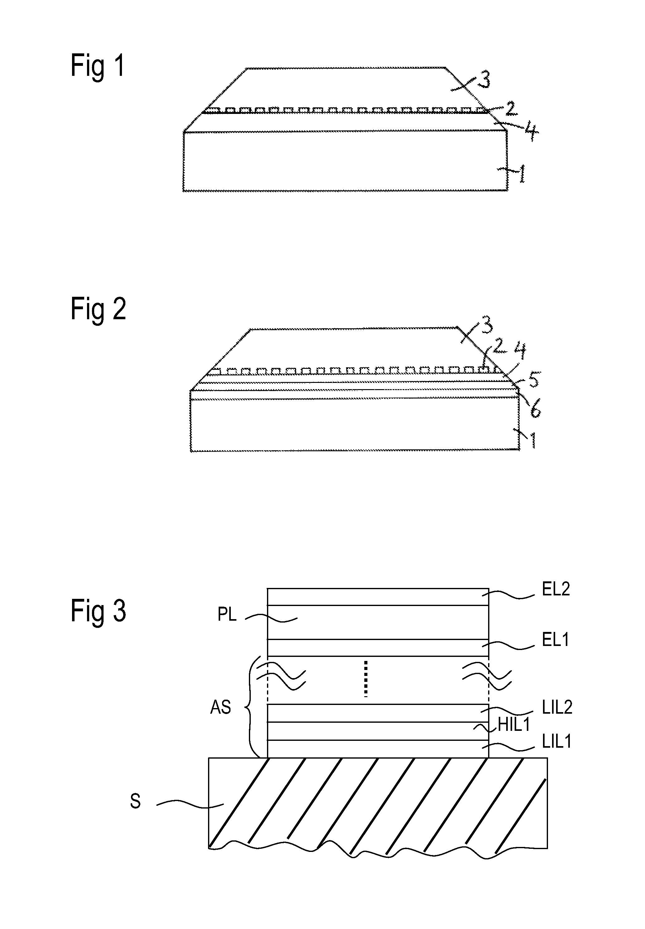
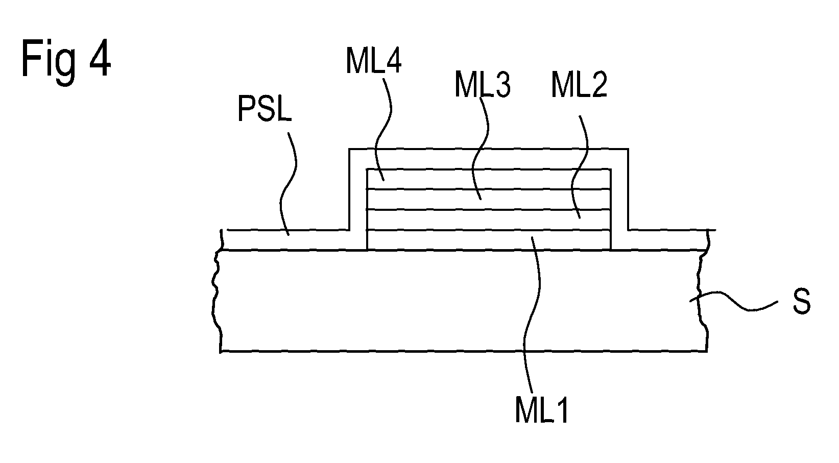
[0046]FIG. 1 shows a schematic cross section through a microacoustic component. A substrate 1 has a layer 4 composed of dielectric or piezoelectric material. The layer 4 can also encompass the entire substrate 1, for example, if the material of the substrate 1 is LiNbO3. A metallic strip structure 2 is arranged on the layer 4, which metallic strip structure can be provided, in particular, for electrodes of the component. The metallic strip structure 2 can be, for example, a plurality of metal strips which are oriented parallel to one another and which are successively alternately connected to a respective connection conductor and in this way form two electrodes intermeshed with one another in a comb-like manner. By way of example, a surface wave component or surface wave filter can be formed with electrodes of this type. In the example illustrated in FIG. 1, the metallic strip structure 2 is covered on the top side with a covering layer 3, which can be a dielectric material, for exa...


PUM

PropertyMeasurementUnit
thicknessaaaaaaaaaa
temperatureaaaaaaaaaa
grain sizesaaaaaaaaaa

Abstract

The microacoustic component has a substrate that has at least one layer (composed of a dielectric or piezoelectric material, and a metallic strip structure. The layer is composed of a dielectric or piezoelectric material and / or the metallic strip structure have / has been produced or can be produced by the atomic layer deposition method.

Description

[0001]This application claims priority to German Patent Application 10 2010 036 256.5, which was filed Sep. 3, 2010 and is incorporated herein by reference.TECHNICAL FIELD[0002]The present invention relates to the production of microacoustic components.BACKGROUND[0003]Conventional deposition methods especially thin layer deposition methods such as vapor deposition, sputtering or PECVD (plasma-enhanced chemical vapor deposition) are used in the production of microacoustic components to produce layers and electrodes. Fluctuations in the thickness of the deposited layer occur in this case. A non-uniform material distribution can occur between different wafers, but also on the same wafer. Since characteristic variables of the components, for example the frequency, are sensitively dependent on the layer thickness, the narrow specifications required are fulfilled only by a small proportion of the components thus produced, unless further complicated process steps are carried out.[0004]If d...

Claims


Application Information

Patent Timeline
Patent Type & Authority Patents(United States)
IPC IPC(8): B05D5/12C23C16/44H01L41/23H01L41/29H01L41/316H03H3/02
CPCH03H3/02H01L41/23H01L41/29H01L41/316H10N30/02H10N30/06H10N30/076
Inventor EGGS, CHRISTOPHHENN, GUDRUNRUILE, WERNERSCHEINBACHER, GUENTERMENZEL, SIEGFRIEDSPINDLER, MARIO
Owner SNAPTRACK
Why Eureka
Try Eureka