Process for obtaining an array of nanodots

a nanodot and nanocrystal technology, applied in the field of nanocrystal production, can solve the problems of poor control of the evolution of these dots, and the deformation of metallic dots used in the floating gates of transistors, so as to improve the behavior of nanodots, improve the performance of mosfet transistors, and maintain the behavior of dots obtained according to the invention.

Inactive Publication Date: 2015-01-27
COMMISSARIAT A LENERGIE ATOMIQUE ET AUX ENERGIES ALTERNATIVES +2
View PDF11 Cites 4 Cited by
  • Summary
  • Abstract
  • Description
  • Claims
  • Application Information

AI Technical Summary

Benefits of technology

[0023]In particular, it turned out that the metallic dots used in the floating gates of transistors are indeed often degraded by the subsequent steps of finalization of the device, such as a transistor, in which these dots are integrated. These subsequent steps involve elevated temperatures, which may modify the electrical behavior and even the structure of certain dots. The invention provides for obtaining silicidated dots, which therefore are not exclusively metallic. It was found that their behavior is much less sensitive to temperature elevations than is that of purely metallic dots. The behavior of the dots obtained according to the invention therefore remains stable. The process according to the invention therefore makes it possible to improve control of the behavior of nanodots.
[0024]In addition, and in particularly advantageous manner, the process according to the invention makes it possible to improve, very significantly, the control in particular of the height of the dots compared with the known processes for obtaining nanodots.
[0025]As it happens, during development of the invention, it was found that the variability of electrical behavior of silicidated nanodots often results from a lack of homogeneity of silicidation phases possible between silicon and metal. It was also found that this lack of homogeneity results from the variation of the ratio of quantity of metal provided to quantity of silicon contained in each of the dots. To control this ratio, the invention discloses a method that reduces the dispersion in particular of the height and therefore of the volume of the nanocrystals before silicidation, as well as the spacing thereof. The dispersion of the size of the nanocrystals is reduced. The quantity of metal to be provided can therefore be precisely determined, and the ratio of quantity of metal provided to quantity of silicon contained in each of the dots is better controlled. The result is dots having improved and more predictable electrical behavior.
[0026]In this way the invention makes it possible to improve significantly the performances and reproducibility of devices in which these nanocrystals are integrated.
[0027]For example, it permits fine and reproducible control of the trapping of charges in a floating gate. Consequently, it is particularly well adapted to the obtaining of memory cells that permit programming of several information bits.
[0032]In the context of development of the invention, it turned out that the metallic dots used in the floating gates of transistors are quite often degraded by the subsequent steps of finalization of the device, such as a transistor, in which these dots are integrated. These subsequent steps involve elevated temperatures, which may modify the electrical behavior and even the structure of certain dots. The invention provides for the obtaining of silicidated dots; these dots therefore are not exclusively metallic. It was found that their behavior is much less sensitive to temperature elevations than is that of purely metallic dots. The behavior of the dots obtained according to the invention therefore remains stable. The method according to the invention therefore makes it possible to improve control of the behavior of nanodots, thus augmenting the performances of MOSFET transistors in which nanodots are integrated.

Problems solved by technology

In the context of development of the invention, it was found that the variability of the electrical behavior of devices using nanodots results from poor control of the evolution of these dots in the course of obtaining the device.
In particular, it turned out that the metallic dots used in the floating gates of transistors are indeed often degraded by the subsequent steps of finalization of the device, such as a transistor, in which these dots are integrated.

Method used


Image

  • Process for obtaining an array of nanodots
  • Process for obtaining an array of nanodots
  • Process for obtaining an array of nanodots

Examples


Embodiment Construction

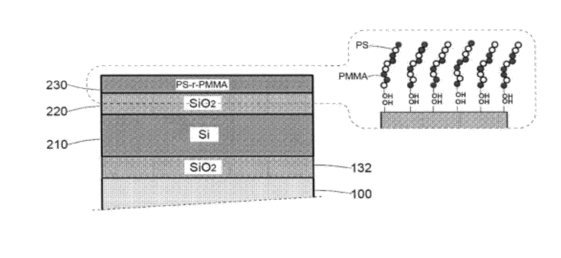
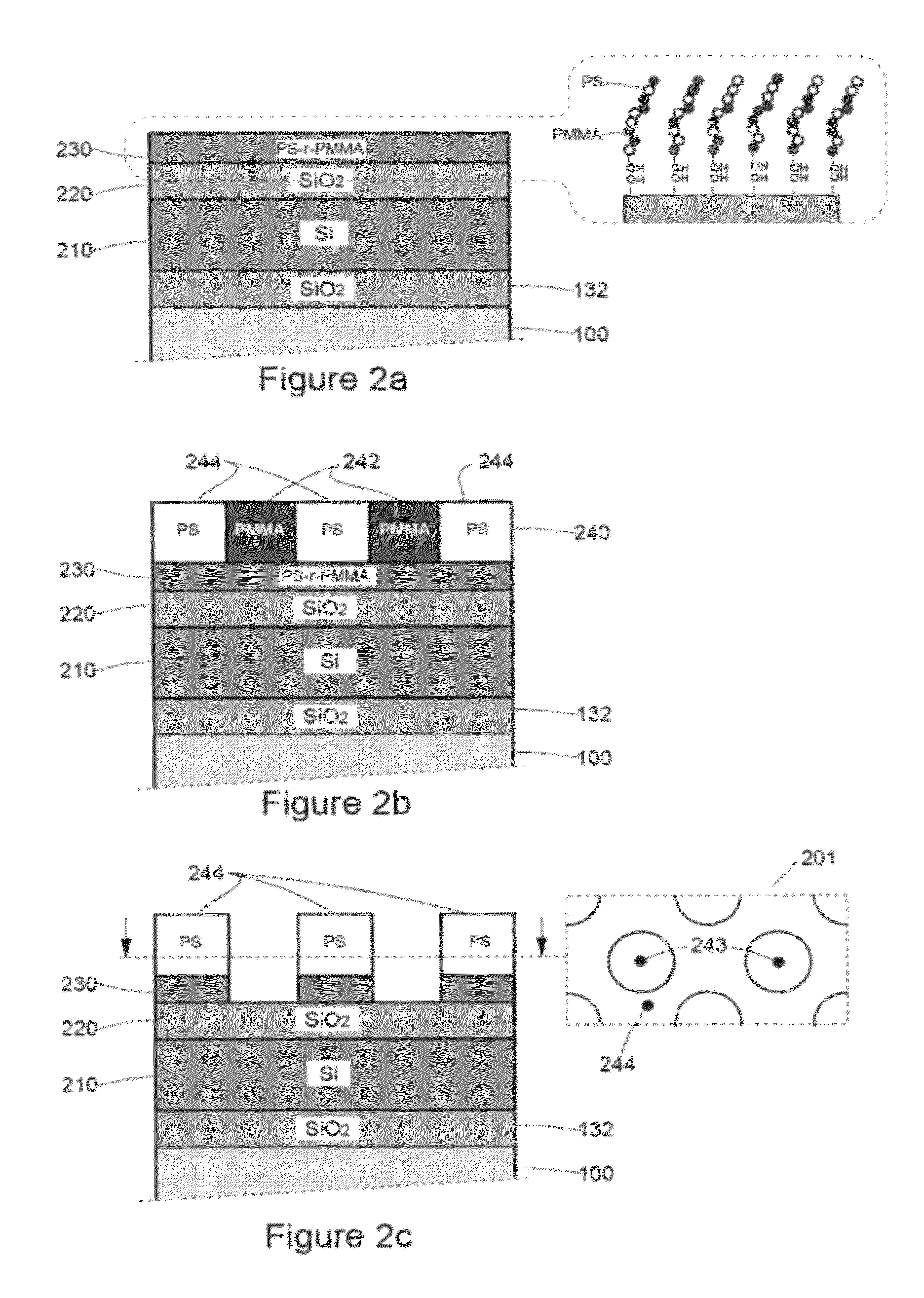
[0041]Before a detailed description of the invention is presented, it is recalled that it describes a method for obtaining an array of nanodots for microelectronic devices comprising the following steps: deposition of a silicon layer on a substrate; formation, above the silicon layer, of a layer of a material capable of self-organizing, in the interior of which at least one polymer substantially forms cylinders organized into an array within a matrix; formation of patterns in the layer of a material capable of self-organizing by elimination of the said cylinders; formation of a mask by transfer of the said patterns; production of silicon dots in the silicon layer by engraving with the mask; silicidation of the silicon dots, comprising deposition of a metal layer.

[0042]Optionally, the invention may additionally comprise at least any one of the following optional characteristics:

[0043]Preferably, the silicon layer is a layer of polycrystalline silicon. Alternatively, the silicon layer...


PUM

PropertyMeasurementUnit
thicknessaaaaaaaaaa
thicknessaaaaaaaaaa
thicknessaaaaaaaaaa

Abstract

A process for obtaining an array of nanodots (212) for microelectronic devices, characterized in that it comprises the following steps:deposition of a silicon layer (210) on a substrate (100, 132),formation, above the silicon layer (210), of a layer (240) of a material capable of self-organizing, in which at least one polymer substantially forms cylinders (242) organized into an array within a matrix (244),formation of patterns (243) in the layer (240) of a material capable of self-organizing by elimination of the said cylinders (242),formation of a hard mask (312) by transfer of the said patterns (243),production of silicon dots (212) in the silicon layer (210) by engraving through the hard mask (312),silicidation of the silicon dots (212), comprising deposition of a metal layer (510).

Description

TECHNICAL FIELD OF THE INVENTION[0001]The present invention relates to the production of nanocrystals of metallic character, especially with a view to forming the floating gate of MOSFET transistors used by non-volatile memories of the EEPROM and FLASH types.PRIOR ART[0002]The constantly progressing miniaturization of devices produced by the microelectronics industry demands that it be possible to construct the basic components, essentially transistors, which from now on will be measured in tens of nanometers (nm=10−9 meter). Consequently the limits of numerous techniques used by this industry, especially those of photolithography, are being reached. To be able to define progressively smaller patterns with very great precision at the surface of a semiconductor substrate, photolithography must implement increasingly more sophisticated means, such as, for example, the use of shorter wavelengths, into the ultraviolet, for exposure of photosensitive resins through masks reproducing the ...

Claims


Application Information

Patent Timeline
Patent Type & Authority Patents(United States)
IPC IPC(8): H01L21/20H01L21/28H01L21/308H01L29/423H01L29/788
CPCH01L21/28273H01L21/3081H01L21/3086H01L29/42332H01L29/7881H01L29/40114
Inventor GAY, GUILLAUMEBARON, THIERRYJALAGUIER, ERIC
Owner COMMISSARIAT A LENERGIE ATOMIQUE ET AUX ENERGIES ALTERNATIVES
Why Eureka
Try Eureka