Packaging substrate having embedded through-via interposer and method of fabricating the same

a technology of through-via interposer and packaging substrate, which is applied in the direction of resistive material coating, solid-state device coating, metallic material coating process, etc., can solve the problems of reducing product reliability, porous and brittle low-k dielectric material, etc., to improve product reliability, reduce the thickness of the overall structure, and crack the effect of solder bumps

Active Publication Date: 2015-02-03
UNIMICRON TECH CORP
View PDF6 Cites 6 Cited by
  • Summary
  • Abstract
  • Description
  • Claims
  • Application Information

AI Technical Summary

Benefits of technology

[0013]According to the present invention, first end surfaces of the conductive through-vias of the through-via interposer electrically connect with the redistribution layer to thereby electrically connect to electrode pads of a semiconductor chip having smaller pitches, and second end surfaces of the conductive through-vias electrically connect with the conductive vias of the built-up structure having larger pitches, thereby allowing the packaging substrate to be coupled with the semiconductor chip having high-density circuits. Therefore, the present invention overcomes the conventional drawback of mismatch between packaging substrates and semiconductor chips having high-density circuits without changing original supply chains and infrastructures of IC industries.
[0014]Further, if a semiconductor chip is disposed on the through-via interposer, since the CTEs of the through-via interposer and the semiconductor chip are close to each other, cracking of solder bumps between the semiconductor chip and the through-via interposer is prevented, thereby effectively improving the product reliability.
[0015]Furthermore, the present invention embeds the through-via interposer in the encapsulant layer so as to reduce the thickness of the overall structure. In addition, since the built-up structure is formed on the second surface of the encapsulant layer, the present invention eliminates the need of a core board as in the prior art, which also facilitates reduction of the thickness of the overall structure.

Problems solved by technology

However, such a low-k dielectric material is porous and brittle.
Therefore, during a thermal cycling test for reliability characterization of the flip-chip packaging structure, the solder bumps 11 easily crack due to uneven thermal stresses caused by a significant difference between the thermal expansion coefficients (CTE) of the packaging substrate 10 and the semiconductor chip 12, thereby easily causing the semiconductor chip 12 to crack and hence reducing the product reliability.
However, the flip-chip bonding pads 100 of the packaging substrate 10 are of micro-scale pitches, which do not match the high-density nano-scale circuits of the semiconductor chip 12.

Method used


Image

  • Packaging substrate having embedded through-via interposer and method of fabricating the same
  • Packaging substrate having embedded through-via interposer and method of fabricating the same
  • Packaging substrate having embedded through-via interposer and method of fabricating the same

Examples


Embodiment Construction

[0020]The following illustrative embodiments are provided to illustrate the disclosure of the present invention, these and other advantages and effects can be apparent to those in the art after reading this specification.

[0021]It should be noted that all the drawings are not intended to limit the present invention. Various modification and variations can be made without departing from the spirit of the present invention. Further, terms, such as “one,”“on,”“top,”“bottom,” etc., are merely for illustrative purpose and should not be construed to limit the scope of the present invention.

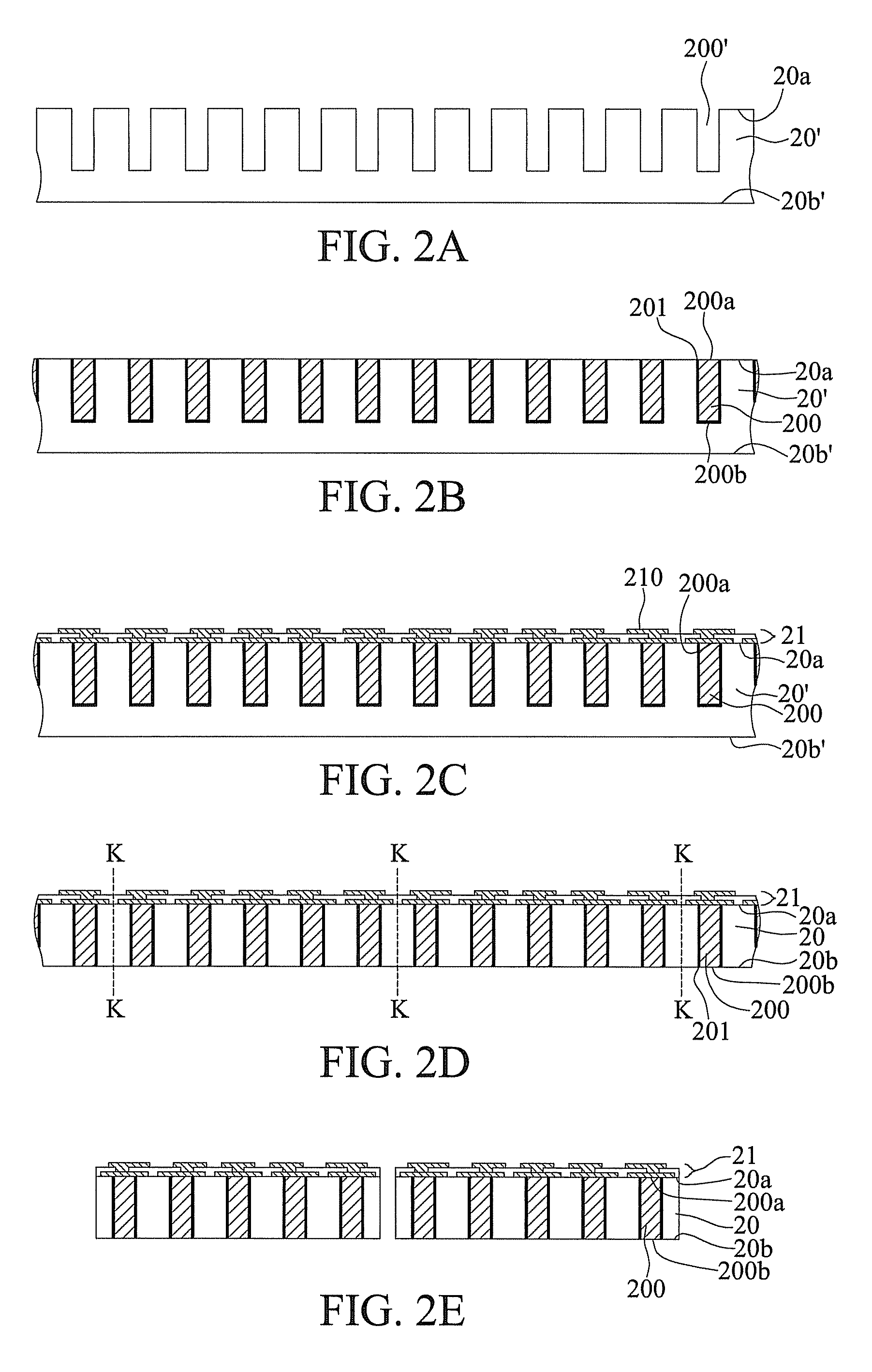
[0022]FIGS. 2A to 2J are schematic cross-sectional views illustrating a method of fabricating a packaging substrate having an embedded through-via interposer according to a first embodiment of the present invention.

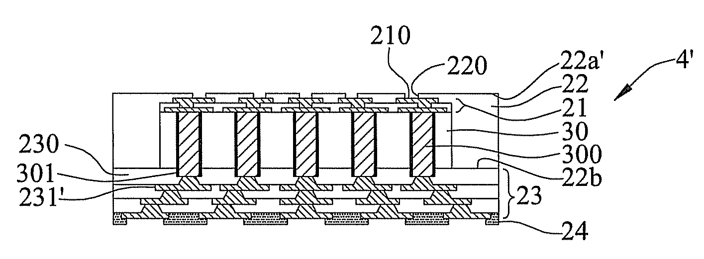
[0023]Referring to FIG. 2A, an interposer 20′ is provided. The interposer 20′ has opposite first side 20a and second side 20b′. A plurality of through-vias 200′ are formed at the first side 20...


PUM

PropertyMeasurementUnit
heightaaaaaaaaaa
conductiveaaaaaaaaaa
electrical performanceaaaaaaaaaa

Abstract

A packaging substrate having an embedded through-via interposer is provided, including an encapsulant layer, a through-via interposer embedded in the encapsulant layer and having a plurality of conductive through-vias therein, a redistribution layer embedded in the encapsulant layer and formed on the through-via interposer so as to electrically connect with first end surfaces of the conductive through-vias, and a built-up structure formed on the encapsulant layer and the through-via interposer for electrically connecting second end surfaces of the conductive through-vias. As such, the first end surfaces of the conductive through-vias are electrically connected to the redistribution layer to thereby be electrically connected to electrode pads of a semiconductor chip having smaller pitches, while the second end surfaces of the conductive through-vias electrically connect with conductive vias of the built-up structure having larger pitches, thereby allowing the packaging substrate to be coupled with the semiconductor chip.

Description

CROSS-REFERENCES TO RELATED APPLICATIONS[0001]This application claims under 35 U.S.C. §119(a) the benefit of Taiwanese Application No. 100139667, filed Oct. 31, 2011, the entire contents of which is incorporated herein by reference.BACKGROUND OF THE INVENTION[0002]1. Field of the Invention[0003]The present invention relates to packaging substrates and methods of fabricating the same, and, more particularly, to a packaging substrate having an embedded through-via interposer for carrying a semiconductor chip and a method of fabricating the same.[0004]2. Description of Related Art[0005]FIG. 1 is a schematic cross-sectional view of a conventional flip-chip package structure. In fabrication, a bismaleimide-triazine (BT) packaging substrate 10 that has a core board 102, a first surface 10a and a second surface 10b is provided, and a plurality of flip-chip bonding pads 100 are formed on the first surface 10a of the packaging substrate 10; the flip-chip bonding pads 100 are electrically con...

Claims


Application Information

Patent Timeline
Patent Type & Authority Patents(United States)
IPC IPC(8): H05K1/00H01L21/48H01L23/14H01L23/15H01L23/498
CPCH01L21/4846H01L23/147H01L23/15H01L23/49822H01L23/49827H01L2924/15311H01L23/49816H01L2224/131H01L2224/16237H01L2224/73204H01L2224/32225H01L2224/16225H01L2924/00014H01L2924/014Y10T29/4913Y10T29/49146Y10T29/49165H01L23/48H01L21/76898H05K1/11H05K1/112H05K1/142H05K1/183H05K3/4038H05K2201/10674
Inventor HU, DYI-CHUNGTSENG, TZYY-JANG
Owner UNIMICRON TECH CORP
Why Eureka
Try Eureka