Eureka AIR delivers breakthrough ideas for toughest innovation challenges, trusted by R&D personnel around the world.

Resistive memory device and fabrication methods

Active Publication Date: 2015-02-03
CROSSBAR INC
View PDF242 Cites 1 Cited by
  • Summary
  • Abstract
  • Description
  • Claims
  • Application Information

AI Technical Summary

Benefits of technology

The patent describes a type of memory that can be used in processors and other devices. These memories are non-volatile, meaning they can remember their data even when power is turned off. This improves the devices' performance and reduces power consumption. These memories are different from CMOS type memories, which need to be refreshed regularly to maintain their data. The patent is directed towards devices that use these memory devices, such as smartphones and network devices.

Problems solved by technology

However, as field effect transistors (FETs) approach sizes less than 100 nm, physical problems such as short channel effect begin to hinder proper device operation.
For transistor based memories, such as those commonly known as Flash memories, other performance degradations or problems may occur as device sizes shrink.
With Flash memories, a high voltage is usually required for programming of such memories, however, as device sizes shrink, the high programming voltage can result in dielectric breakdown and other problems.
Similar problems can occur with other types of non-volatile memory devices other than Flash memories.
A common drawback with these memory devices include that they often require new materials that are incompatible with typical CMOS manufacturing.
As another example of this, Fe-RAM and MRAM devices typically require materials using a high temperature anneal step, and thus such devices cannot be normally be incorporated with large volume silicon-based fabrication techniques.
Additional drawbacks with these devices include that such memory cells often lack one or more key attributes required of non-volatile memories.
As an example of this, Fe-RAM and MRAM devices typically have fast switching (e.g. “0” to “1”) characteristics and good programming endurance, however, such memory cells are difficult to scale to small sizes.
In another example of this, for ORAM devices reliability of such memories is often poor.
As yet another example of this, switching of PCRAM devices typically includes Joules heating and undesirably require high power consumption.

Method used


Image

  • Resistive memory device and fabrication methods
  • Resistive memory device and fabrication methods
  • Resistive memory device and fabrication methods

Examples


Embodiment Construction

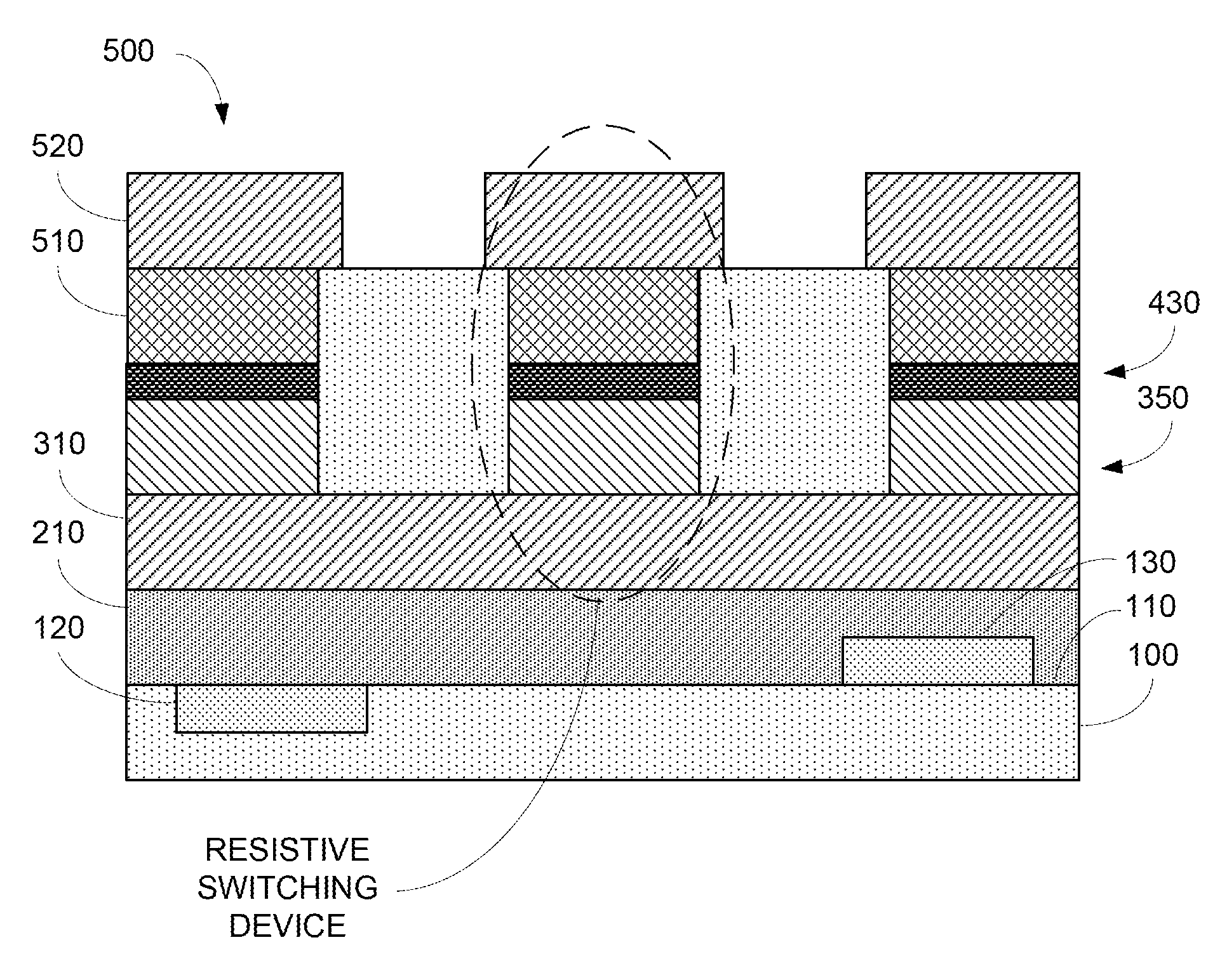
[0023]The present invention is generally related to a memory (switching) device and an apparatus including a memory device. More particularly, embodiments of the present invention provide structures and a methods for forming one or more resistive switching / memory devices each having improved memory retention characteristics. The embodiments described herein are described with respect to fabrication of high density non-volatile memory devices. However, one of ordinary skill in the art will recognize that these devices may be applied to a broad range of applications, such as processing devices, computing devices, or the like.

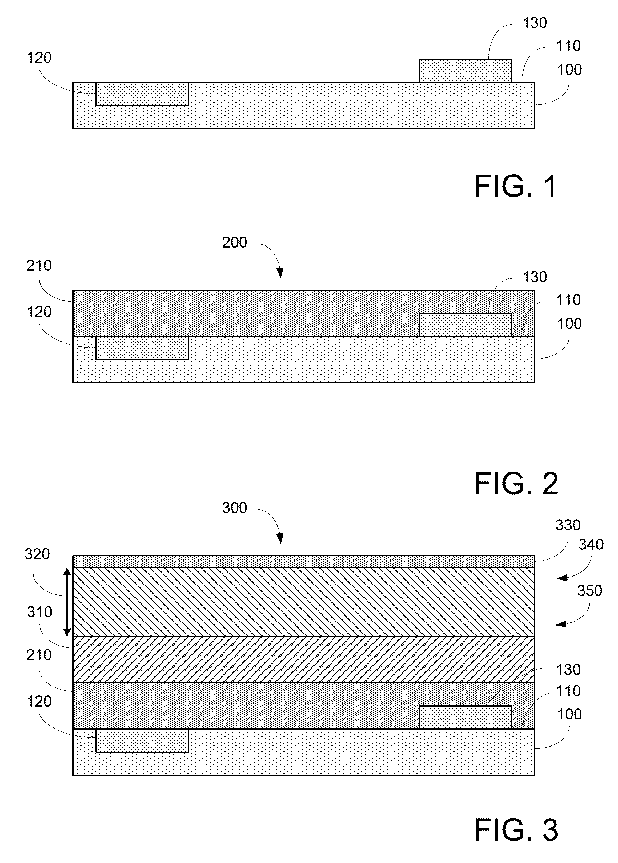
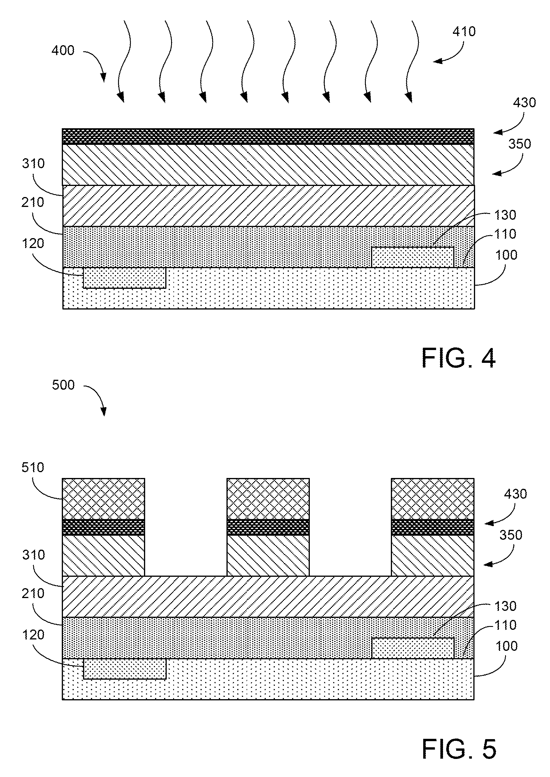
[0024]FIG. 1 illustrates a substrate 100 having a surface region 110. In various embodiments, the substrate 100 can be a semiconductor substrate, such as: a single crystal silicon wafer, a silicon germanium wafer, a silicon-on-insulator substrate, commonly known as SOI, and the like.

[0025]Depending on the specific embodiment, the processes described herein are bac...


PUM


Abstract

A method for forming a resistive memory device includes providing a substrate comprising a first metal material, forming a conductive silicon-bearing layer on top of the first metal material, wherein the conductive silicon-bearing layer comprises an upper region and a lower region, and wherein the lower region is adjacent to the first metal material, forming an amorphous layer from the upper region of the conductive silicon-bearing layer, and disposing an active metal material above the amorphous layer.

Description

CROSS-REFERENCE TO RELATED CASES[0001]The present invention claims priority to and is a non-provisional of Ser. No. 61 / 620,561 filed Apr. 5, 2012. That application is herein by incorporated by reference for all purposes.BACKGROUND[0002]The present invention relates to memory devices. More particularly, the present invention discloses non-volatile resistive switch memory devices having improved operational characteristics, fabrication techniques, as well as apparatus including such memories.[0003]The inventor of the present invention has recognized the success of semiconductor devices has been mainly driven by an intensive transistor down-scaling process. However, as field effect transistors (FETs) approach sizes less than 100 nm, physical problems such as short channel effect begin to hinder proper device operation. For transistor based memories, such as those commonly known as Flash memories, other performance degradations or problems may occur as device sizes shrink. With Flash me...

Claims


Application Information

Patent Timeline
IPC IPC(8): H01L29/02
CPCH10B63/30H10B63/80H10N70/245H10N70/841H10N70/884H10N70/883H10N70/826H10N70/028H10N70/063H10N70/24
Inventor JO, SUNG HYUNKIM, KUK-HWANKUMAR, TANMAY
Owner CROSSBAR INC
Why Eureka
Eureka Blog
Learn More