Sapphire substrate and method for manufacturing the same and nitride semiconductor light emitting element
a technology of semiconductor light emitting elements and semiconductor substrates, which is applied in the direction of polycrystalline material growth, crystal growth process, after-treatment details, etc., can solve problems such as crystal defects becoming apparen
- Summary
- Abstract
- Description
- Claims
- Application Information
AI Technical Summary
Benefits of technology
Problems solved by technology
Method used
Image
Examples
example 1
[0077]Hereinafter, Examples with respect to embodiments of the present invention are described.
[0078]The projections were formed on a sapphire substrate by the following procedures.
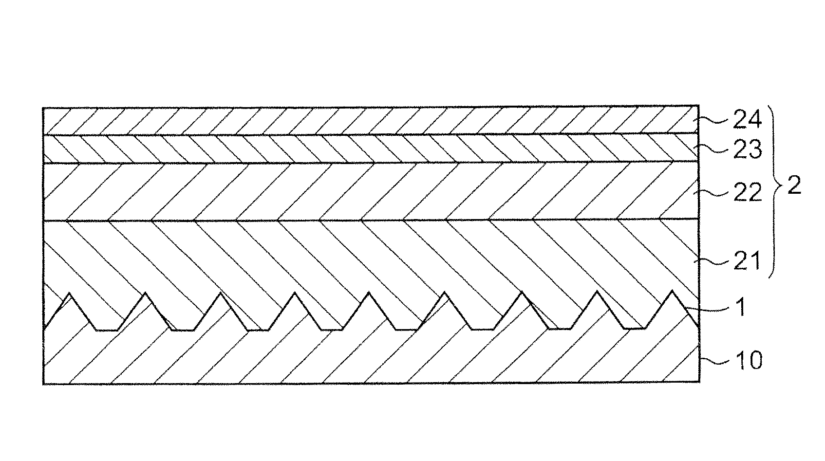
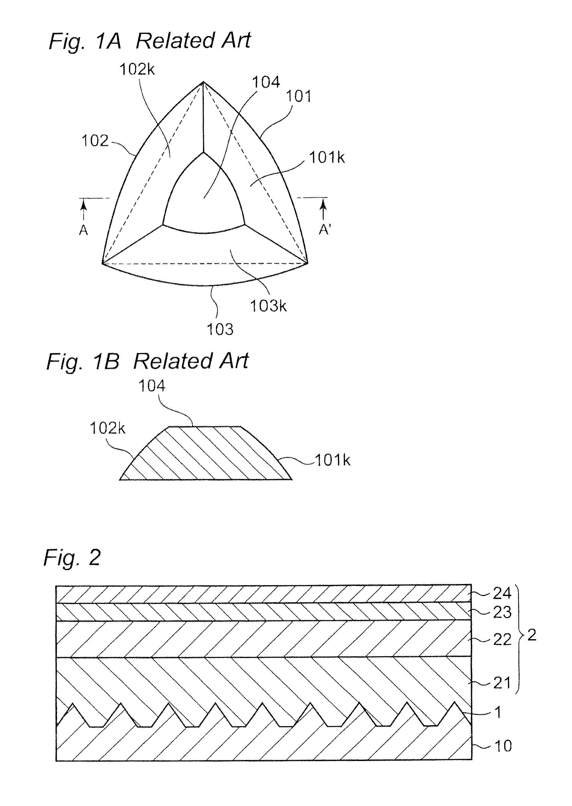
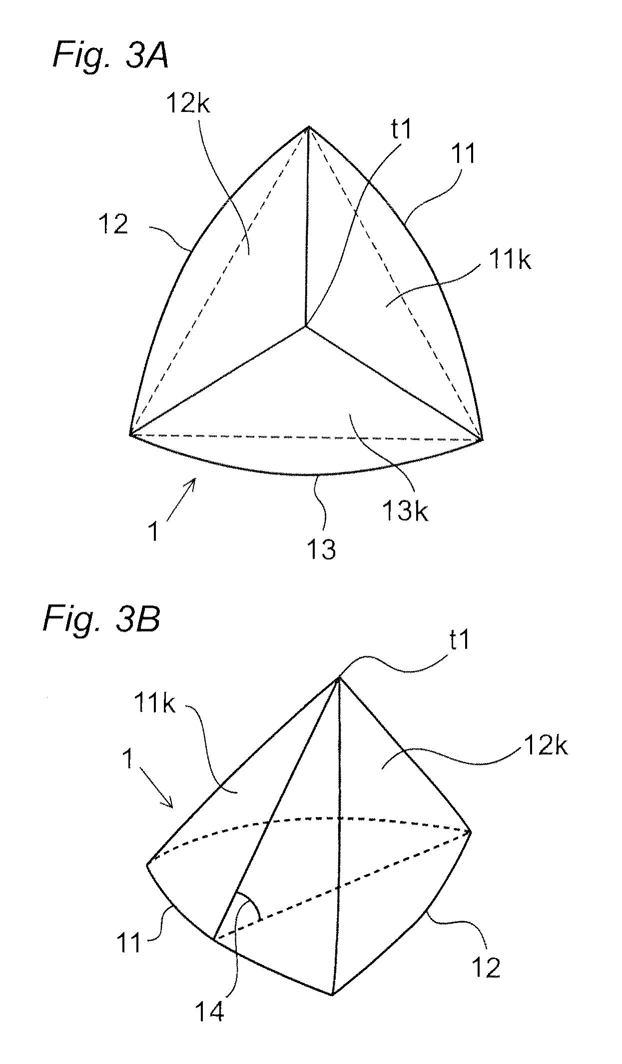
[0079]A plurality of circular-shaped etching masks having diameters of about 1.5 μm were formed on each vertex of triangular lattice with a side of 1.9 μm by forming SiO2 layer on a C-plane (0001) of the sapphire substrate and by patterning the SiO2 layer. Subsequently, the substrate was immersed in an etching bath using a mixed acid of phosphoric acid and sulfuric acid as an etching liquid and etched with the solution temperature of about 290° C. for about 5 minutes. By this, a plurality of projections having substantially triangular pyramidal-shape with a pointed top were formed on the sapphire substrate. The inclined angle of the side surfaces constituting the projections was about 54°, the height of the projections was about 1.2 μm, the distance between the projections was 2.1 μm, and C-plane area rat...
example 2
[0096]Then, nitride semiconductor light emitting elements of Example 2 and Comparative Example 2 were prepared which had the distance between the projections of between 1.9 and 3.1 μm and C-plane area ratio of between about 35% and 70% by the similar procedures to those explained in Example 1 and Comparative Example 1 described above. These nitride semiconductor light emitting elements of Example 2 and Comparative Example 2 have the same constitution as those of Example 1 and Comparative Example 1 described above except that the distance between the projections was between 1.9 and 3.1 μm and C-plane area ratio was between about 35% and 70%.
[0097][Measurement of Luminous Flux]
[0098]Bullet-shaped light emitting devices were prepared using the obtained light emitting elements of Example 2 and Comparative Example 2, similarly to Example 1 and Comparative Example 1 described above. Each of the prepared light emitting devices of Example 2 and Comparative Example 2 was placed at the center...
example 3
[0103]A nitride semiconductor light emitting elements of Example 3 which had the distance between the projections of 2.5 μm and C-plane area ratio of 51% was prepared by the similar procedures to those of the above-described Example 1. This nitride semiconductor light emitting elements of Example 3 had the same configuration as that of Example 1 except that the distance between the projections was 2.5 μm and C-plane area ratio was 51%.
PUM
| Property | Measurement | Unit |
|---|---|---|
| inclination angle | aaaaa | aaaaa |
| inclination angle | aaaaa | aaaaa |
| height | aaaaa | aaaaa |
Abstract
Description
Claims
Application Information
 - R&D
- Intellectual Property
- Life Sciences
- Materials
- Tech Scout
- Unparalleled Data Quality
- Higher Quality Content
- 60% Fewer Hallucinations
Browse by: Latest US Patents, China's latest patents, Technical Efficacy Thesaurus, Application Domain, Technology Topic, Popular Technical Reports.
© 2025 PatSnap. All rights reserved.Legal|Privacy policy|Modern Slavery Act Transparency Statement|Sitemap|About US| Contact US: help@patsnap.com


