Ohmic contact to semiconductor layer

a technology of ohmic contact and semiconductor layer, which is applied in the field of ohmic contact, can solve the problems of deteriorating device performance, difficult to grow well doped p-type gan with a carrier concentration of more than 10

Active Publication Date: 2015-03-03
SENSOR ELECTRONICS TECH
View PDF19 Cites 10 Cited by
  • Summary
  • Abstract
  • Description
  • Claims
  • Application Information

AI Technical Summary

Problems solved by technology

A drawback of the recessed source and drain contacts is a presence of a short channel effect, which can deteriorate the device performance.
Making a p-type contact to p-type GaN, for example, is much more difficult.
In particular, it is difficult to grow well doped p-type GaN with a carrier concentration of more than 1018 cm−3 due to a high activation energy of acceptors.
Additionally, it is difficult to find metals with a work function that corresponds to p-type GaN.
In addition, use of superlattices, strained semiconductor layers, and spontaneous polarization have been employed to achieve a high hole concentration and result in a low contact resistivity.

Method used


Image

  • Ohmic contact to semiconductor layer
  • Ohmic contact to semiconductor layer
  • Ohmic contact to semiconductor layer

Examples


Embodiment Construction

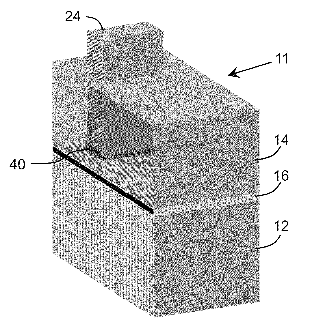
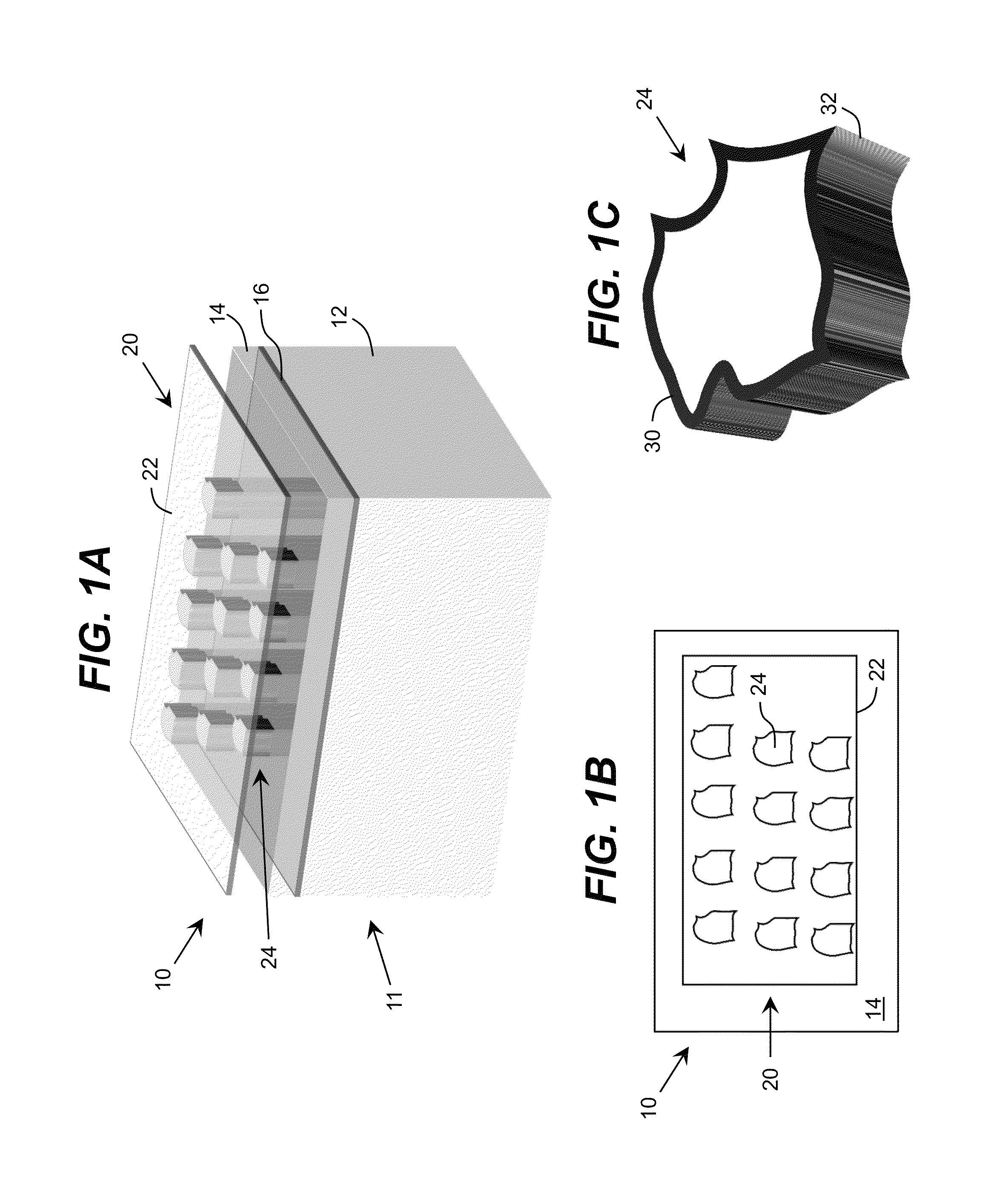
[0030]As indicated above, aspects of the invention provide a perforating ohmic contact to a semiconductor layer in a semiconductor structure. The perforating ohmic contact can include a set of perforating elements, which can include a set of metal protrusions laterally penetrating the semiconductor layer(s). The perforating elements can be separated from one another by a characteristic length scale selected based on a sheet resistance of the semiconductor layer and a contact resistance per unit length of a metal of the perforating ohmic contact contacting the semiconductor layer. The structure can be annealed using a set of conditions configured to ensure formation of the set of metal protrusions. As used herein, unless otherwise noted, the term “set” means one or more (i.e., at least one) and the phrase “any solution” means any now known or later developed solution.

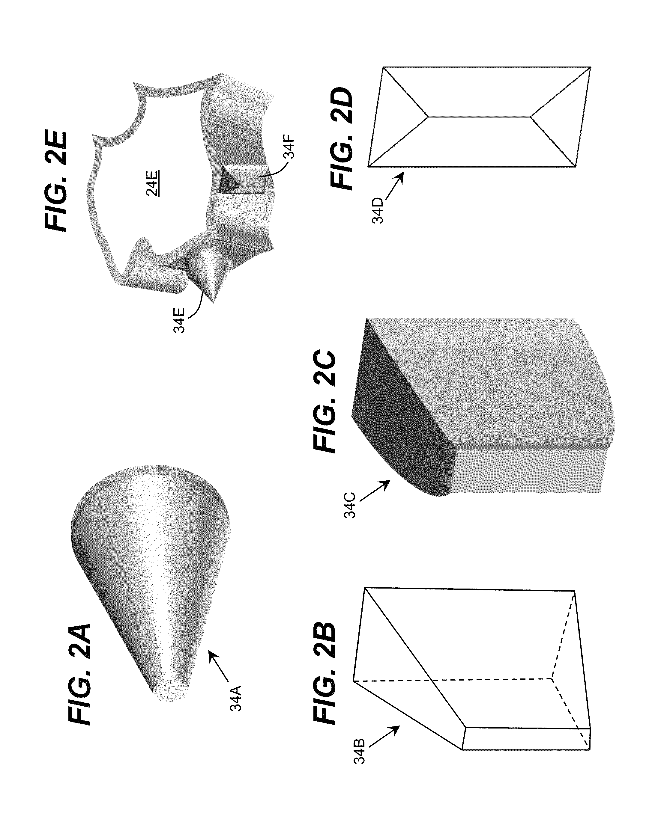
[0031]A perforating ohmic contact described herein includes a plurality of perforating elements, which penetrate (e.g....


PUM


Abstract

A perforating ohmic contact to a semiconductor layer in a semiconductor structure is provided. The perforating ohmic contact can include a set of perforating elements, which can include a set of metal protrusions laterally penetrating the semiconductor layer(s). The perforating elements can be separated from one another by a characteristic length scale selected based on a sheet resistance of the semiconductor layer and a contact resistance per unit length of a metal of the perforating ohmic contact contacting the semiconductor layer. The structure can be annealed using a set of conditions configured to ensure formation of the set of metal protrusions.

Description

REFERENCE TO RELATED APPLICATIONS[0001]The current application claims the benefit of U.S. Provisional Application No. 61 / 655,437, titled “Ohmic Contact to Semiconductor Layers,” which was filed on 4 Jun. 2012, and which is hereby incorporated by reference.TECHNICAL FIELD[0002]The disclosure relates generally to ohmic contacts, and more particularly, to an improved method of manufacturing an ohmic contact to a semiconductor layer.BACKGROUND ART[0003]Developing a good ohmic contact to a semiconductor layer is critical for the operation, stability, and lifetime of the corresponding semiconductor device. Various approaches have been employed to form ohmic contacts. One approach, which can produce a good ohmic contact to a semiconductor layer, uses an annealing process. For example, titanium / aluminum (Ti / Al) is frequently used as an ohmic contact to n-doped nitride semiconductor layers. In this case, a titanium nitride (TiN) layer creates N vacancies in the underlying aluminum gallium ni...

Claims


Application Information

Patent Timeline
Patent Type & Authority Patents(United States)
IPC IPC(8): H01L21/44H01L21/768H01L29/20H01L29/45
CPCH01L21/768H01L29/2003H01L29/452H01L21/28575H01L21/28587H01L21/28593H01L29/4175H01L29/41766H01L33/38H01L2933/0016
Inventor GAEVSKI, MIKHAILSIMIN, GRIGORYSHATALOV, MAXIM SDOBRINSKY, ALEXANDERSHUR, MICHAELGASKA, REMIGIJUS
Owner SENSOR ELECTRONICS TECH
Why Eureka
Try Eureka