NVSRAM cells with voltage flash charger

a technology of nvsram cells and flash chargers, applied in the field of n, can solve the problems of the large size of the 12t nmos nvsram memory, and achieve the effects of large overhead, long channel length, and large number of transistors

Inactive Publication Date: 2015-03-10
APLUS FLASH TECH
View PDF29 Cites 4 Cited by
  • Summary
  • Abstract
  • Description
  • Claims
  • Application Information

AI Technical Summary

Benefits of technology

[0019]Note, the way to short the drains nodes and source nodes is not to use metal with a active contact that will create too much parasitic capacitance with an impact of reducing flash cell threshold level difference ΔVt between the paired Flash transistors. The preferred way is to make the N-active connection between two separate source nodes and drain nodes of the paired NMOS Flash Charger transistor like forming a NMOS capacitor with the active layer enclosure full poly gate of the Flash Charger.
[0020]The shorted drains and sources nodes of one pair of Flash Charger transistors would increase sharing of the coupling-generated charges from both Flash Charger transistor channels when a common gate voltage PumpWL of the pair of Flash Charger transistors is ramped up to a desired voltage, which is above VDD but lower than VPP. As a result, the final data node voltage difference ΔVQ-QB is almost doubled over the above version with Source and Drain nodes totally separated for a superior Recall operation.
[0027]In an alternative embodiment, the present invention provides that channel length of each Flash transistor can be flexibly increased to generate more coupling HV charges to Q and QB nodes for ensuring the success of the voltage follower operation.
[0028]In another alternative embodiment, the present invention provides that gate voltage of each Flash transistor can be flexibly increased to the highest level of VPP to generate more coupling charges below Mch1 and Mch2 with a shorter channel length for area reduction.
[0029]In yet another alternative embodiment, the present invention provides that gate voltage of Flash word line, FWL, can be flexibly increased from a negative value to a highest level of maximum Vt level, preferred to be positive, of the Flash transistors to help generate coupling charges for a DRAM-like charge-sensing scheme. In other words, more charges differences at paired Q and QB nodes can be achieved by taking the ramp gate of FWL on the flash transistors with a ΔVt.
[0040]During NVSRAM's Recall operation, the flash part of this pseudo-10T NVSRAM cell is configured into a paired voltage followers with their respective drain voltages preferably supplied by the coupling-generated charges rather than by the current supply from the VDD pin. As a result, the number of transistors used in each Flash string can be reduced from 3T to 2T without a bottom HV Select transistor that has a big overhead of a long channel length. Thus, the pseudo-10T NVSRAM cell can gain another 15% or more in cell size saving.

Problems solved by technology

One big drawback of this 12T NMOS NVSRAM memory is its large 12T cell size that comprises one 6T LV SRAM cell and one 6T HV Flash cell.

Method used


Image

  • NVSRAM cells with voltage flash charger
  • NVSRAM cells with voltage flash charger
  • NVSRAM cells with voltage flash charger

Examples


Embodiment Construction

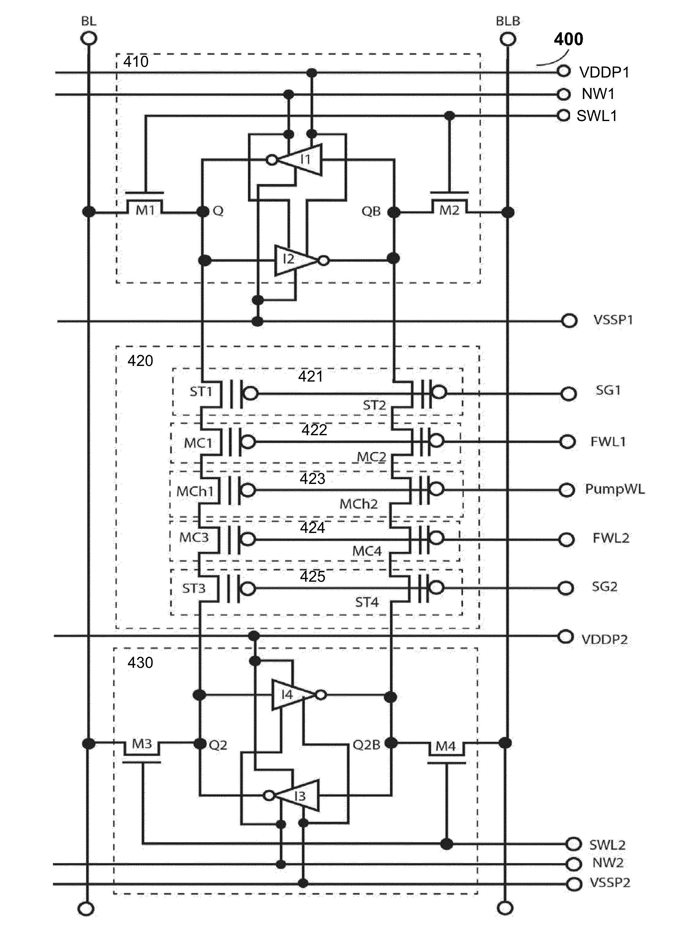
[0051]The present invention relates to a preferred 12T NVSRAM cell with a Flash Charger or a pseudo-10T NVSRAM cell comprising one LV 6T SRAM cell, one 4T Flash cell and one shared paired Flash Charger transistors (2T) that can be made of a conventional 2-poly Flash transistor or a 1-poly Select transistor by shorting poly2 and poly1 of the flash cell. These shared 2T Flash Charger transistors are formed on available room of layout spacing between two source nodes of two 10T NVSRAM cells laid in same column without taking extra silicon area. Thus, this preferred pseudo-10T NVSRAM cell makes a cell size of the 12T NVSRAM cell with a Flash Charger effectively equivalent to a 10T cell.

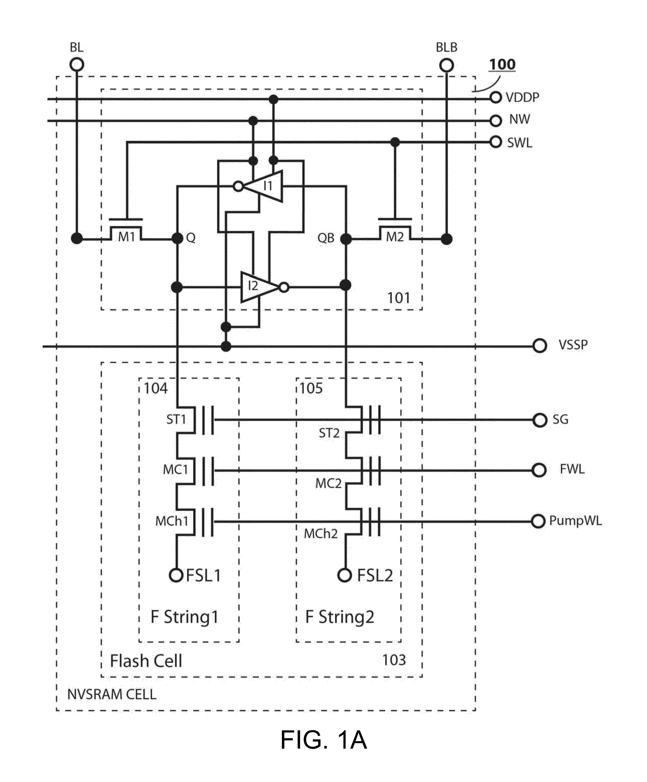
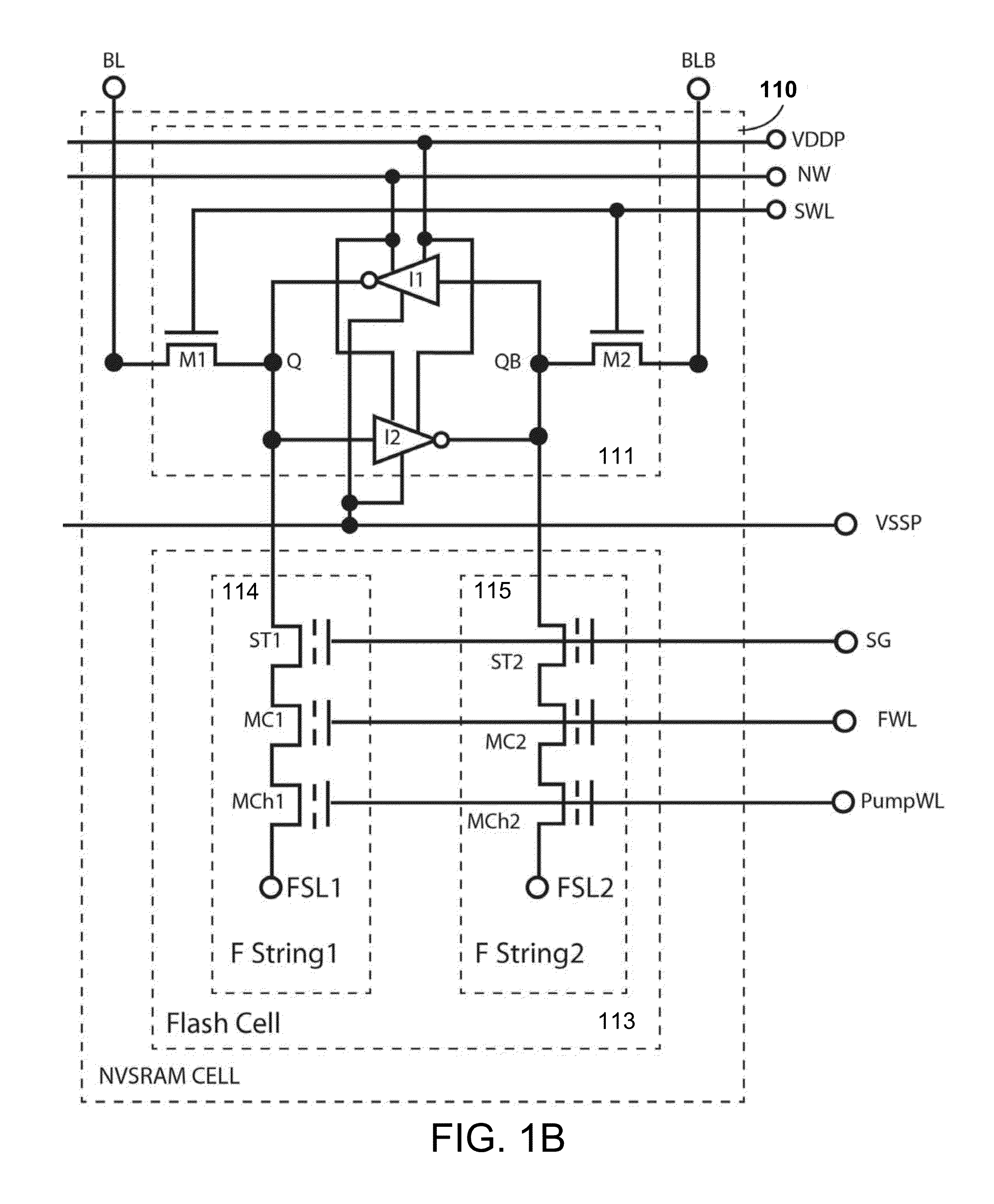
[0052]FIG. 1A shows a preferred embodiment of a 2-poly NMOS 12T NVSRAM cell with a Flash-based Charger of the present invention. Each 12T NVSRAM cell with a Flash Charger 100 includes one 6T LV SRAM cell 101 and one 6T NMOS 2-poly Flash cell 103. Each 6T LV SRAM cell 101 is like conventional one having tw...


PUM


Abstract

The present invention discloses two preferred embodiments of a 12T NVSRAM cell with a flash-based Charger and a pseudo 10T NVSRAM cell with one shared Flash-based Charger. The Flash-based Charger can be made of a 2-poly floating-gate type or a 1-poly charge-trapping SONOS / MONOS flash type, regardless of PMOS type or NMOS type. In an alternative embodiment, the Store operation of above two preferred NVSRAM cell use a DRAM-like charge-sensing scheme with Flash cell configured into a voltage follower associated with Flash Charger and 2-step SRAM amplification technique to amplify the threshold level difference ΔVt stored in the paired Flash transistors. The ΔVt can be detected as low as 1V when the coupled charges through the Flash charger are sufficient by ramping a gate control of the Flash Charger as high as VPP or by increasing the channel length for the Flash Charger.

Description

CROSS-REFERENCE TO RELATED APPLICATIONS[0001]This application claims priority to U.S. Patent Application No. 61 / 721,467, filed on Nov. 1, 2012, commonly assigned, and hereby incorporated by references in their entireties herein for all purposes.[0002]This application is related to U.S. Pat. No. 7,164,608, U.S. patent application Ser. Nos. 14 / 037,356, 14 / 053,549, 14 / 058,227, 14 / 059,618, and 14 / 064,220, commonly assigned, which are incorporated by reference herein for all purposes.[0003]Additionally, this application is related to U.S. Pat. No. 7,760,540.TECHNICAL FIELD OF THE INVENTION[0004]The present invention relates to a 12T NVSRAM cell with a flash Charger comprising one LV 6T SRAM cell, one 4T Flash cell and one shared paired Flash Charger transistors (2T) that can be made of a conventional 2-poly Flash transistor or a 1-poly Select transistor by shorting poly2 and poly1 of the flash cell. Additionally, the invention also provides a pair of mirrored 10T NVSRAM cells with a shar...

Claims


Application Information

Patent Timeline
Patent Type & Authority Patents(United States)
IPC IPC(8): G11C11/34G11C14/00
CPCG11C14/0063
Inventor LEE, PETER WUNG
Owner APLUS FLASH TECH
Why Eureka
Try Eureka