Method of forming an array of high aspect ratio semiconductor nanostructures

a technology of semiconductor nanostructures and arrays, which is applied in the field of forming arrays of high aspect ratio semiconductor nanostructures, can solve problems such as uniformity and scalability, and achieve the effect of high aspect ratio

Active Publication Date: 2015-03-17
THE BOARD OF TRUSTEES OF THE UNIV OF ILLINOIS
View PDF10 Cites 12 Cited by
  • Summary
  • Abstract
  • Description
  • Claims
  • Application Information

AI Technical Summary

Problems solved by technology

However, uniformity and scalability remain as challenges for the bottom-up growth paradigm.

Method used


Image

  • Method of forming an array of high aspect ratio semiconductor nanostructures
  • Method of forming an array of high aspect ratio semiconductor nanostructures
  • Method of forming an array of high aspect ratio semiconductor nanostructures

Examples


examples

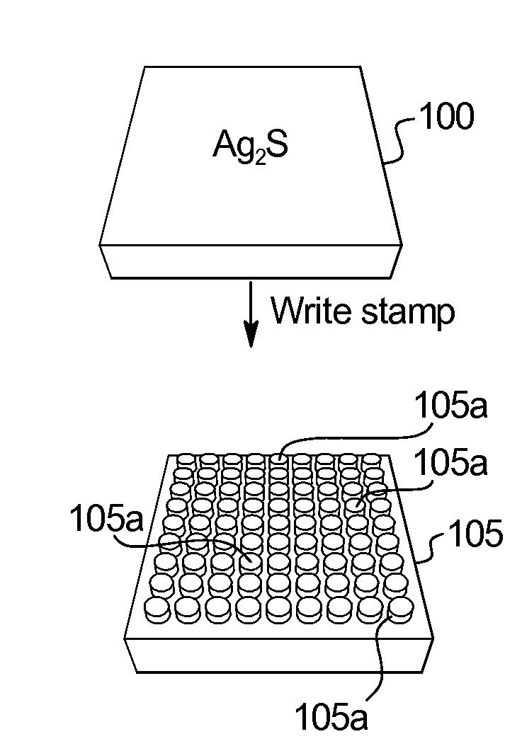
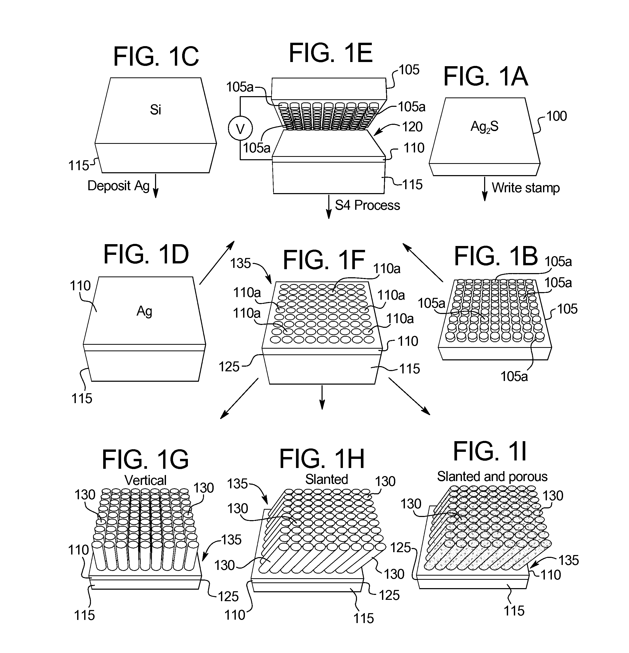
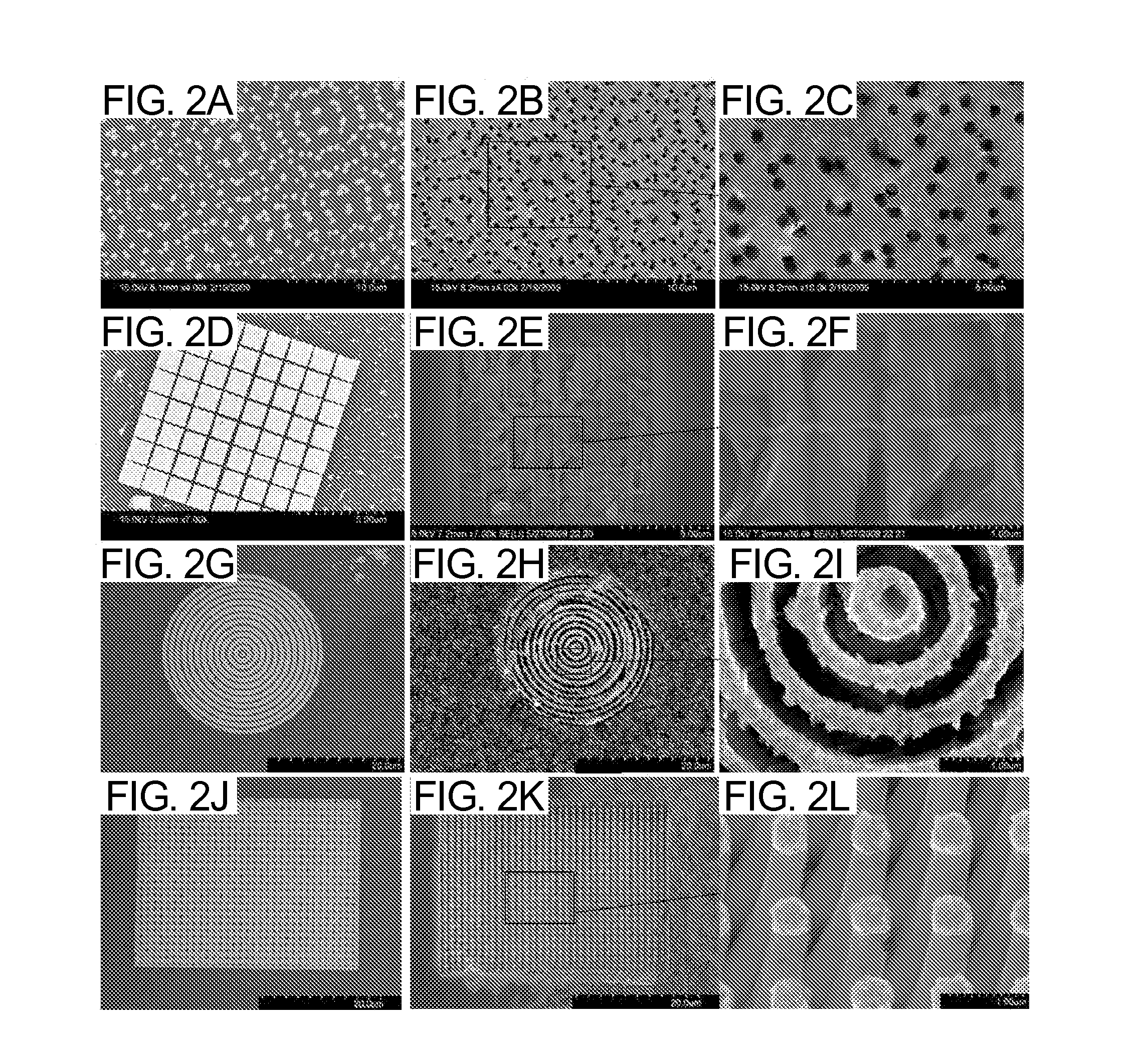
[0042]In the following examples, S4 is combined with MacEtch to fabricate large area silicon nanowire arrays and other high aspect ratio nanostructures with controlled morphological and optical properties. The focus is S4 patterning of silver nanoscale metallic patterns on silicon wafers and subsequent metal-assisted chemical etching in a HF and H2O2 solution. Through spatially resolved optical spectroscopy and imaging using cathodoluminescence (CL), emission in the red, green and blue color range resulting from Si nanowire structures is demonstrated. The emission may be tuned by varying the etching solution concentration, etching time, and crystal orientation. Furthermore, through the removal of the silver pattern and re-deposition of a silver film on the silicon nanowires, a plasmonic enhancement of the blue emission is verified. The advantages of the S4 and MacEtch combination and the unique features of the nanostructures produced using this technique, as well as potential applic...


PUM

PropertyMeasurementUnit
sizeaaaaaaaaaa
surface roughnessaaaaaaaaaa
ionic conductivityaaaaaaaaaa

Abstract

A new method for forming an array of high aspect ratio semiconductor nanostructures entails positioning a surface of a stamp comprising a solid electrolyte in opposition to a conductive film disposed on a semiconductor substrate. The surface of the stamp includes a pattern of relief features in contact with the conductive film so as to define a film-stamp interface. A flux of metal ions is generated across the film-stamp interface, and a pattern of recessed features complementary to the pattern of relief features is created in the conductive film. The recessed features extend through an entire thickness of the conductive film to expose the underlying semiconductor substrate and define a conductive pattern on the substrate. The stamp is removed, and material immediately below the conductive pattern is selectively removed from the substrate. Features are formed in the semiconductor substrate having a length-to-width aspect ratio of at least about 5:1.

Description

FEDERALLY SPONSORED RESEARCH OR DEVELOPMENT[0001]The invention described herein is based at least in part upon work supported by the National Science Foundation under NSF Award #0749028 (CMMI) for The Center for Nanoscale Chemical-Electrical-Mechanical Manufacturing Systems. The U.S. Government has certain rights in this invention.RELATED APPLICATIONS[0002]The present patent document is the national stage of International Application No. PCT / US2010 / 052581, which was filed on Oct. 14, 2010, and which claims the benefit of the filing date under 35 U.S.C. §119(e) of U.S. Provisional Patent Application Ser. No. 61 / 253,700, which was filed on Oct. 21, 2009, both of which are hereby incorporated by reference in the entirety.[0003]U.S. patent application Ser. No. 12 / 122,967, which was filed on May 19, 2008, U.S. patent application Ser. No. 11 / 376,908, which was filed on Mar. 16, 2006, International Patent Application No. PCT / US2007 / 064132, which was filed on Mar. 16, 2007, and Internationa...

Claims


Application Information

Patent Timeline
Patent Type & Authority Patents(United States)
IPC IPC(8): H01L21/00B82Y10/00B82Y40/00H01L21/308H01L29/06
CPCH01L21/3081B82Y10/00H01L21/3086H01L29/0676B82Y40/00Y10S977/893
Inventor LI, XIULINGFANG, NICHOLAS X.FERREIRA, PLACID M.CHERN, WINSTONCHUN, IK SUHSU, KENG HAO
Owner THE BOARD OF TRUSTEES OF THE UNIV OF ILLINOIS
Why Eureka
Try Eureka