Eureka AIR delivers breakthrough ideas for toughest innovation challenges, trusted by R&D personnel around the world.

Method of making a transistor

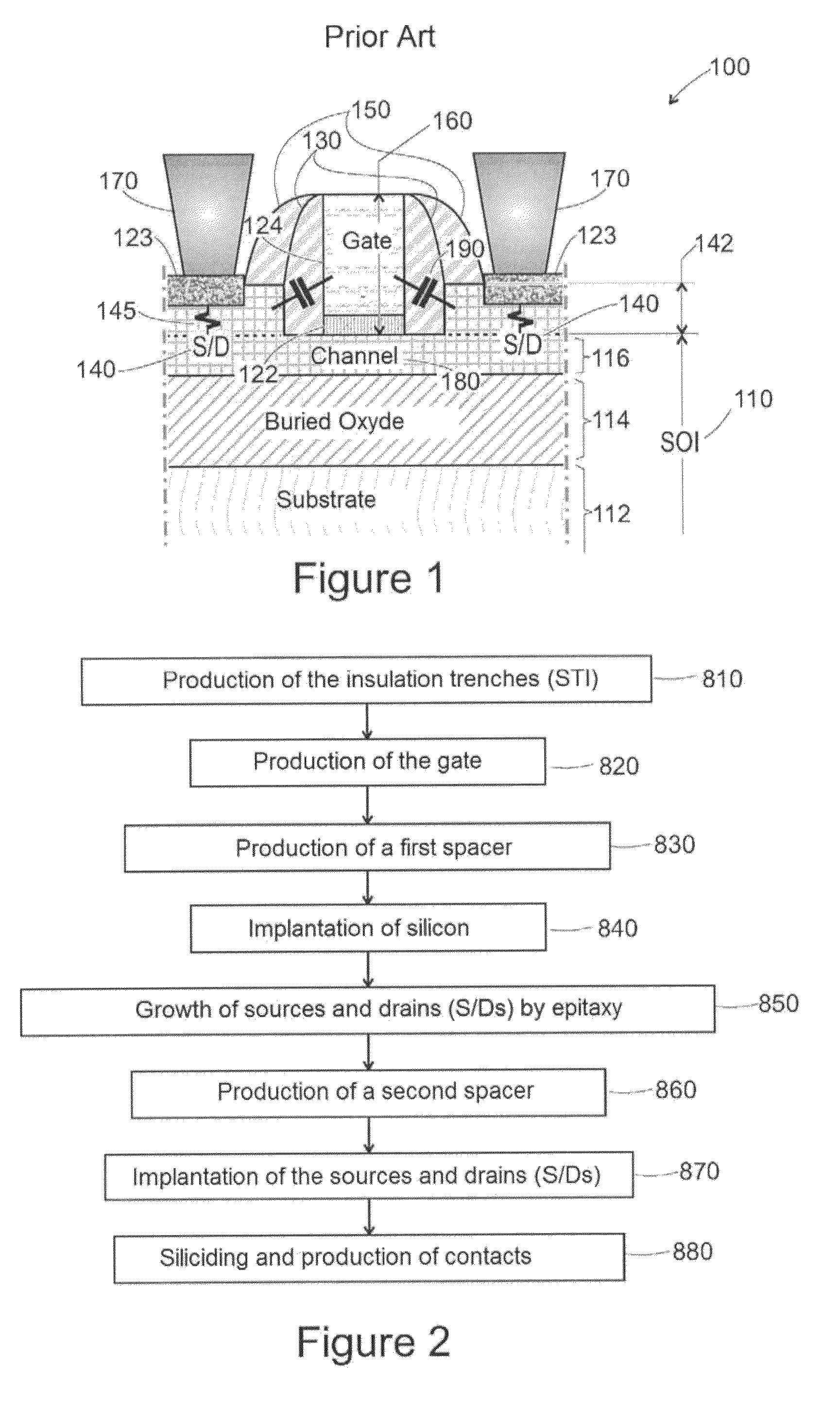
a transistor and transistor technology, applied in the field of transistors, can solve the problems of difficult to precisely control the depth of implantation, and achieve the effects of eliminating alignment defects, simple, reliable and easy to reprodu

Active Publication Date: 2015-03-17
COMMISSARIAT A LENERGIE ATOMIQUE ET AUX ENERGIES ALTERNATIVES +2
View PDF22 Cites 0 Cited by
  • Summary
  • Abstract
  • Description
  • Claims
  • Application Information

AI Technical Summary

Benefits of technology

[0024]Another significant advantage of the present invention lies in the fact that the cavities are formed in the active layer and in the channel by selective etching of the gate. The cavities are thus auto-aligned on the gate. Defects in alignment are therefore eliminated. The method is particularly simple, reliable and easily reproducible.
[0025]Another significant advantage of the present invention lies in the fact that the height of the S / Ds is independent of the thickness of the active layer forming the channel. This advantage is of interest for very many applications and in particular for transistors where the channel has a very low thickness, such as transistors of the FDSOI (fully depleted SOI) type for example. This is because the invention makes it possible to preserve a very thin channel while deciding freely on the S / D height, for example by increasing it for the purpose of reducing the access resistance of the S / Ds without increasing the parasitic capacitance between S / D and gate.
[0026]The invention thus makes it possible to thus propose a particularly effective solution for solving the following problem: offering a solution for reducing the access resistance of the electrodes of the S / Ds without degrading the performance of the transistor, particularly in terms of speed.
[0027]The present invention is particularly suited to substrates of the semiconductor on insulator type, such as elaborate substrates of the silicon on insulator (SOI) type with a thin buried oxide layer (buried insulating oxide, BOX). In a case with a thin buried oxide layer, it is intended for the thickness of the buried oxide layer to be between 145 and 5 nm (nanometers), preferably between 25 and 5 nm without this being limitative. The advantage of the invention is that the embodiments do not depend on the thickness of the buried oxide layer. If a reduction in the thickness of the buried oxide layer is required, for example to provide better electrostatics of the transistor, the invention remains perfectly applicable.
[0028]Another subject matter of the present invention concerns a transistor comprising a stack of layers comprising at least and preferably only: an active layer intended to form a channel for the transistor, an insulating layer disposed opposite a lower face of the channel and on an upper face of a substrate, a gate stack turned facing an upper face of the channel and a source and drain disposed on either side of the gate stack and extending at least partially, preferably mainly and even more preferentially entirely, under the upper face of the channel and / or under the gate stack. The source and drain are disposed in cavities situated on either side of the gate stack. The insulating layer forms an uninterrupted layer between the two cavities of the transistor. The insulating layer has a bottom face, the distance of which with respect to a bottom face of the substrate is greater under the gate stack than in the cavities.
[0029]This transistor structure has the advantage of having a source and drain that are not facing the gate while having a thickness of the insulating layer that is as thin as desired under the channel and source and drain insulated from the substrate by dielectric insulation. This thus makes it possible to particularly significantly reduce the stray capacitances between the gate and the source and drain at a minimum, and to thicken the source and drain in a direction perpendicular to the plane of the substrate, which has the effect of reducing the access resistance of the electrodes of the source and drain.

Problems solved by technology

This is because it is difficult to precisely control the depth of an implantation.

Method used


Image

  • Method of making a transistor
  • Method of making a transistor
  • Method of making a transistor

Examples


first embodiment

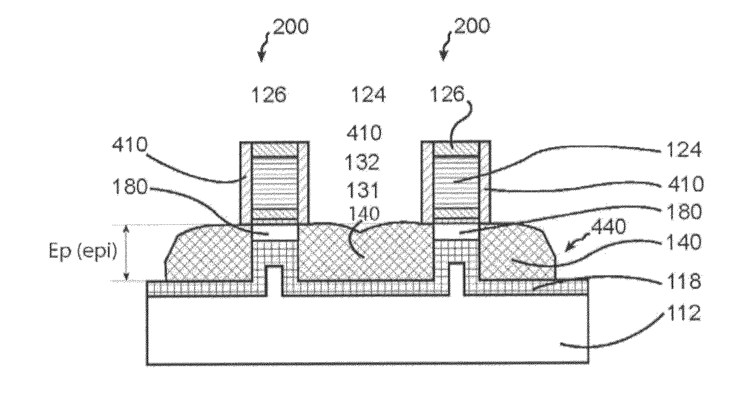
[0120]FIGS. 4a to 4e describe steps of a first embodiment according to the method of the invention.

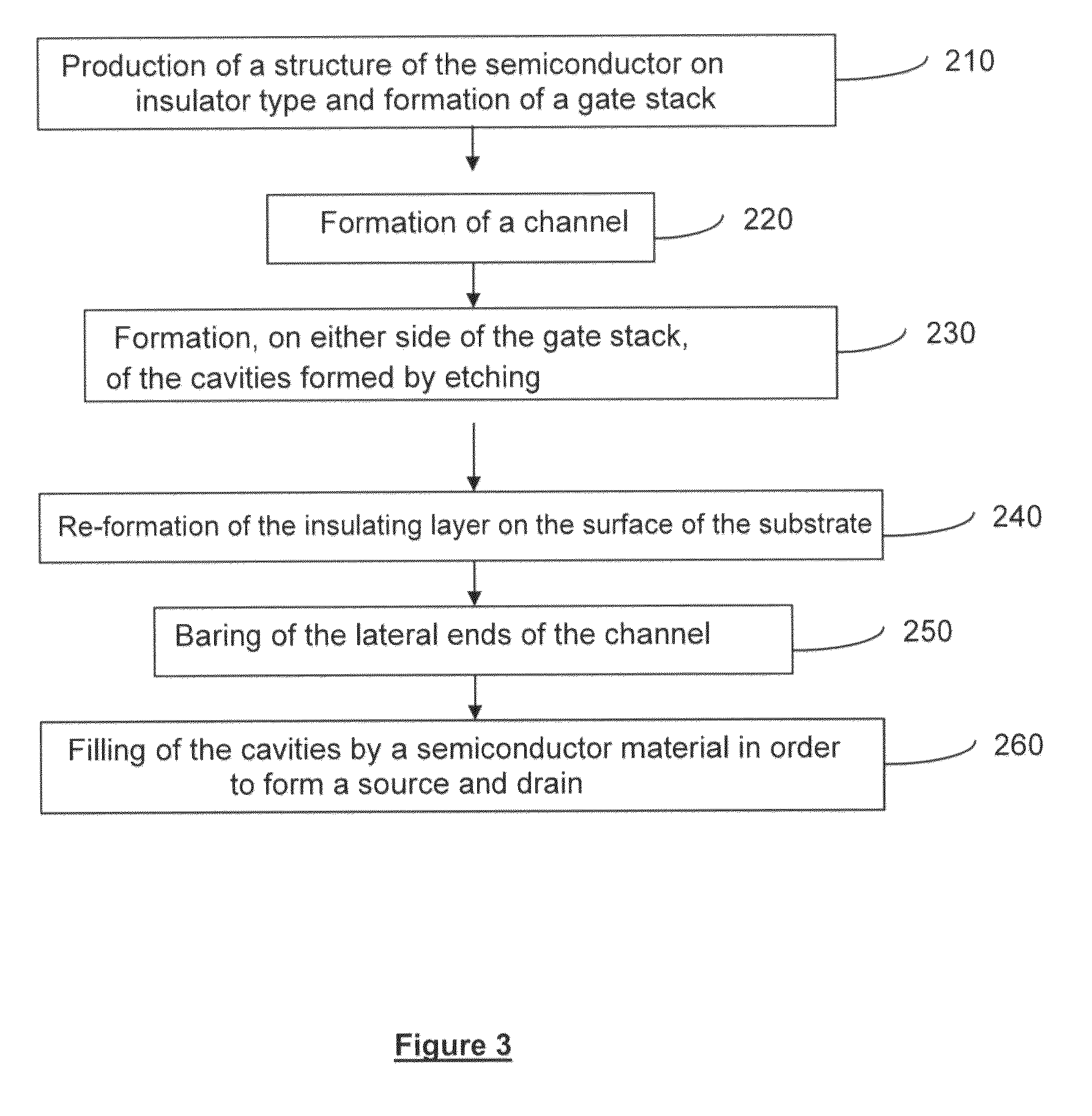
[0121]FIG. 4a illustrates a structure 200 of the SOI type, the active layer 146 of which is surmounted by two gates 124. Only two gates 124 are illustrated in this figure in order to facilitate understanding of the invention. This figure is obtained at the end of step 210 in FIG. 3. This step 210 consists of producing, from a substrate 112, often referred to as a bulk substrate, an initial insulating layer 114 and an active layer 146 intended subsequently to form the channel 180 of each transistor 200. Next, during this step 210, a stack 160 comprising following layers stacked from the active layer 146 is produced: an insulation layer of the gate, often referred to as a thin gate oxide 131 or high-k layer, a metal layer 132, a gate 124 and a hard mask 126 covering the top surface of the gate 124. Furthermore, the substrate 112 is preferentially a doped substrate where the doping level ...

third embodiment

[0135]The oxidation of the surface of the substrate 112 to form the insulating film also leads, in this non-limitative embodiment, to oxidising the portions of the channel 180 that are not protected. This is because the channel 180 is not protected by the spacers 410 or by protective layers, as is the case for example with the third embodiment described below. Advantageously, the oxidation is performed so that the width of the layer of oxide formed on the ends of the channel 180 is at most equal to the width of the spacers 410. For example, the spacers have a width of 10 nm. In addition, the oxidation is performed so that the thickness of the oxidised layer formed on the surface of the substrate 112 is at least twice as great as the width of the layer of oxide formed on the ends of the channel 180. For the gate length of the technological node in question, such as a length of 14 nm or 20 nm, the formation of an oxide as thin as 1 nm at the channel is achievable.

[0136]In the context ...

second embodiment

[0192]FIGS. 7d and 7e show respectively the gate structures at the end of steps 230 and 240. The descriptions concerning these steps are respectively identical to those concerning the performance of steps 230 and 240 of the second embodiment presented respectively in FIGS. 5d and 5e. At the end of these steps, an insulating film is produced on the uncovered surfaces of the substrate 112 in order to re-form, with the remaining portions of the initial insulating layer 114, an uninterrupted insulating layer 118 on the surface of the substrate 112.

[0193]FIG. 7f shows the structure obtained at the end of step 230. In order to have a thicker source and drain 140, a partial step of etching the re-formed insulating layer 118 is performed. This etching is isotropic. The etched thickness is of a dimension at least equal to that of the sacrificial spacers 412.

[0194]Thus the layer of oxide situated in line with the sacrificial spacers 412 is taken off. The etching is performed for example with ...


PUM


Abstract

A method for manufacturing a transistor includes forming a stack of semiconductor on insulator type layers including at least one substrate, surmounted by a first insulating layer and an active layer to form a channel for the transistor; forming a gate stack on the active layer; producing a source and a drain including forming, on either side of the gate stack, cavities by at least one step of etching the active layer, the first insulating layer, and part of the substrate selectively to the gate stack to remove the active layer, the first insulating layer, and a portion of the substrate outside regions situated below the gate stack; forming a second insulating layer on the bared surfaces of the substrate, to form a continuous insulating layer with the first insulating layer; baring of the lateral ends of the channel; and the filling of the cavities by epitaxy.

Description

TECHNICAL FIELD OF THE INVENTION[0001]The present invention relates in general to the transistors of metal oxide semiconductor type with field effects (MOSFET) and more particularly to the reduction of parasitic factors that limit their operating speed and increase their consumption.PRIOR ART[0002]The maximum switching rate of a MOSFET (Metal-Oxide-Semiconductor Field-Effect Transistor) transistor depends on the speed with which the conduction current can be effectively established and made to disappear. Among other factors, it depends on numerous physical parameters specific to the materials used, for example the mobility of carriers of the semiconductor material employed and the levels and type of doping of the different zones defining the electrodes. The switching rate also depends largely on the geometry and structure of the transistors. In particular, by the presence of parasitic factors that are inevitably introduced by the practical manufacture of these devices. Two particula...

Claims


Application Information

Patent Timeline
Patent Type & Authority Patents(United States)
IPC IPC(8): H01L21/00H01L29/66H01L29/78
CPCH01L29/78H01L29/66477H01L29/66772H01L29/78603H01L29/6656H01L29/66636H01L21/84H01L27/1203
Inventor NIEBOJEWSKI, HEIMANUMORAND, YVESVINET, MAUD
Owner COMMISSARIAT A LENERGIE ATOMIQUE ET AUX ENERGIES ALTERNATIVES
Why Eureka
Eureka Blog
Learn More