

Curable silicone composition, cured product thereof, and optical semiconductor device
a technology of silicone composition and curing product, which is applied in the direction of semiconductor devices, solid-state devices, electrical apparatuses, etc., can solve the problems of poor mold releasability, low curing rate, and low mold filling rate, and achieves low discoloration or lowering of mechanical strength, good curing rate, and excellent formability.
- Summary
- Abstract
- Description
- Claims
- Application Information
AI Technical Summary
Benefits of technology
Problems solved by technology
Method used
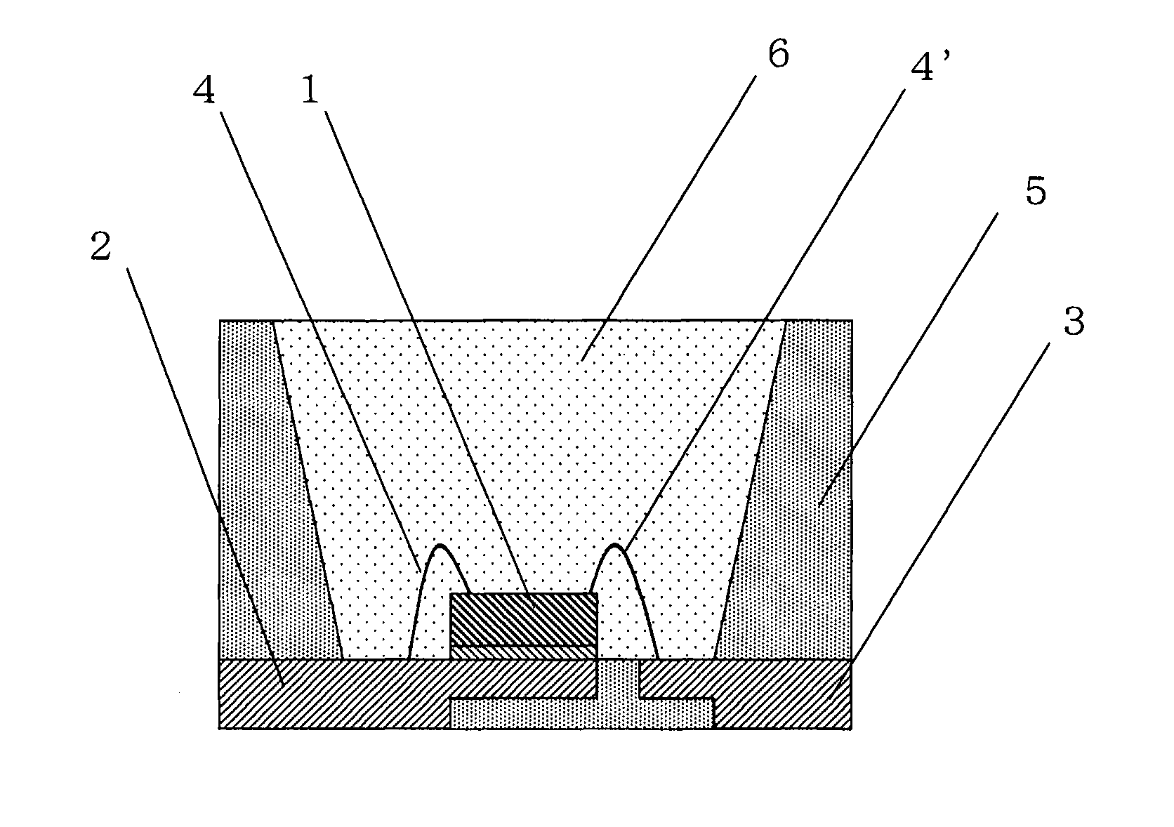
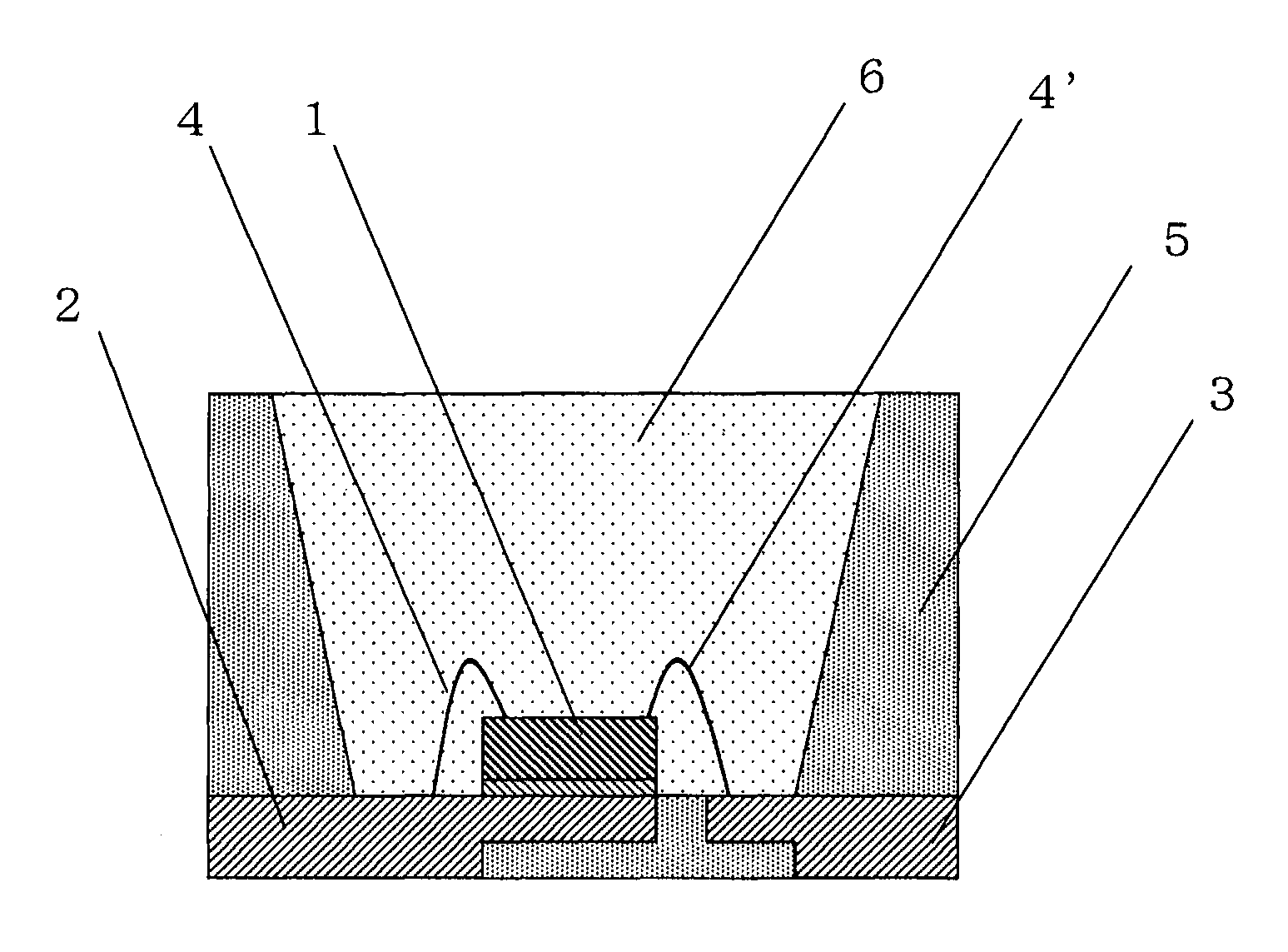
Image

Examples
example 1
Practical Example 1
[0076]100 parts by mass of a methylvinylphenylpolysiloxane represented by the following average unit formula:
(MeViSiO2 / 2)0.15(Me2SiO2 / 2)0.15(Ph2SiO2 / 2)0.30(PhSiO3 / 2)0.40(HO1 / 2)0.04
25 parts by mass of 1,3,5,7-tetramethyl-1,3,5,7-tetravinylcyclotetrasiloxane represented by the following formula:
(MeViSiO)4
2.0 parts by mass of an epoxy group-containing polysiloxane represented by the following average unit formula:
(Me2ViSiO1 / 2)0.2(MeEpSiO2 / 2)0.25(PhSiO3 / 2)0.55(HO1 / 2)0.005
62 parts by mass of 1,1,5,5-tetramethyl-3,3-diphenyltrisiloxane represented by the following formula:
(HMe2SiO)2SiPh2
in an amount that provides 1.0 mole of silicon atom-bonded hydrogen atoms in the present component per 1 mole of the total amount of vinyl groups in the aforementioned methylvinylphenylpolysiloxane, 1,3,5,7-tetramethyl-1,3,5,7-tetravinylcyclotetrasiloxane, and epoxy group-containing polysiloxane, 1,3-divinyl-1,1,3,3-tetramethyldisiloxane solution of 1,3-divinyl-1,1,3,3-tetramethyldis...
example 2
Practical Example 2
[0078]100 parts by mass of a methylvinylphenylpolysiloxane represented by the following average unit formula:
(MeViSiO2 / 2)0.25(Ph2SiO2 / 2)0.3(PhSiO3 / 2)0.45(HO1 / 2)0.4
37.5 parts by mass of phenyltris(dimethylvinylsiloxy)silane represented by the following formula:
(ViMe2SiO)3SiPh
3.0 parts by mass of an epoxy group-containing polysiloxane represented by the following average unit formula:
(Me3SiO1 / 2)0.2(Me2ViSiO1 / 2)0.2(EpSiO3 / 2)0.2(PhSiO3 / 2)0.4(HO1 / 2)0.01
87 parts by mass of 1,1,5,5-tetramethyl-3,3-diphenyltrisiloxane represented by the following formula:
(HMe2SiO)2 SiPh2
in an amount that provides 1.0 mole of silicon atom-bonded hydrogen atoms in the present component per 1 mole of the total amount of vinyl groups in the aforementioned methylvinylphenylpolysiloxane, phenyltris(dimethylvinylsiloxy)silane, and epoxy group-containing polysiloxane, 10 parts by mass of a silicon atom-bonded hydrogen atom-containing methylphenylpolysiloxane represented by the following averag...
example 3
Practical Example 3
[0081]100 parts by mass of a methylvinylphenylpolysiloxane represented by the following average unit formula:
(MeViSiO2 / 2)0.10(Me2SiO2 / 2)0.15(PhSiO3 / 2)0.75(HO1 / 2)0.01
37 parts by mass of tetrakis(dimethylvinylsiloxy)silane represented by the following formula:
Si(OSiMe2Vi)4
6.0 parts by mass of an epoxy group-containing polysiloxane represented by the following average unit formula:
(Me2ViSiO1 / 2)0.2(Ph2SiO2 / 2)0.4(EpSiO3 / 2)0.4
87 parts by mass of 1,1,5,5-tetramethyl-3,3-diphenyltrisiloxane represented by the following formula:
(HMe2SiO)2SiPh2
in an amount that provides 1.1 moles of silicon atom-bonded hydrogen atoms in the present component per 1 mole of the total amount of vinyl groups in the aforementioned methylvinylphenylpolysiloxane, tetrakis(dimethylvinylsiloxy)silane, and epoxy group-containing polysiloxane, 1,3-divinyl-1,1,3,3-tetramethyldisiloxane solution of 1,3-divinyl-1,1,3,3-tetramethyldisiloxane complex of platinum in an amount that provides 3.5 ppm of th...
PUM
| Property | Measurement | Unit |
|---|---|---|
| viscosity | aaaaa | aaaaa |
| bending strength | aaaaa | aaaaa |
| luminous reflectance | aaaaa | aaaaa |
Abstract
Description
Claims
Application Information