

Sintered oxide compact target for sputtering and process for producing the same
a technology of sputtering and compact target, applied in the direction of diaphragms, metallic material coating processes, domestic applications, etc., can solve the problems of increased power consumption, decreased aperture ratio, and malfunction of thin film transistors, so as to reduce the generation of nodules, reduce bulk resistance value, and facilitate dc sputtering
- Summary
- Abstract
- Description
- Claims
- Application Information
AI Technical Summary
Benefits of technology
Problems solved by technology
Method used
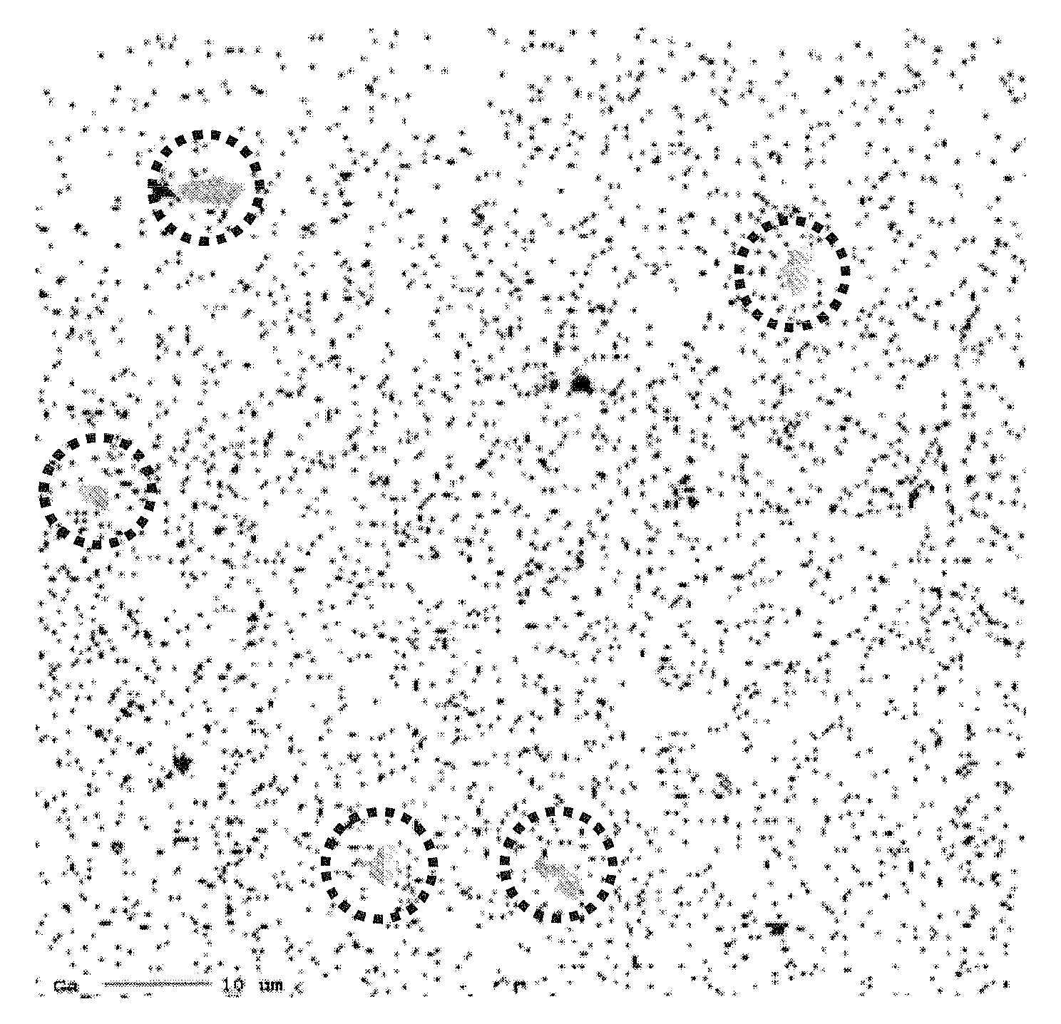
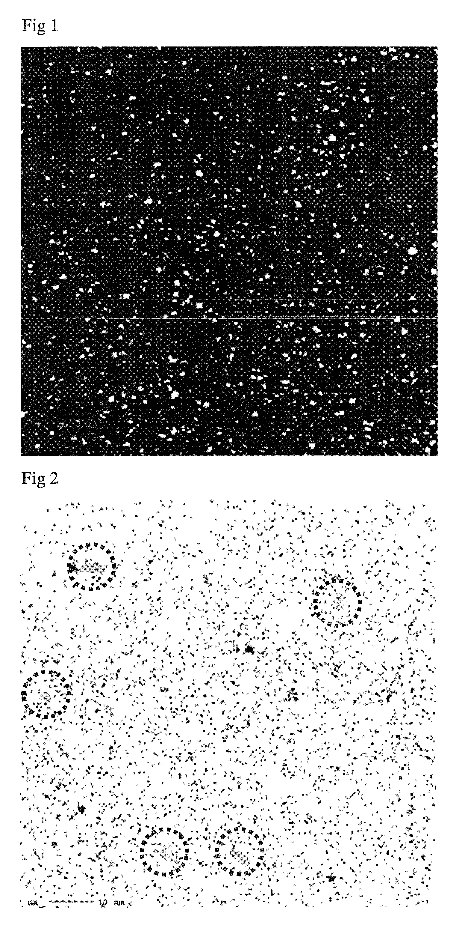
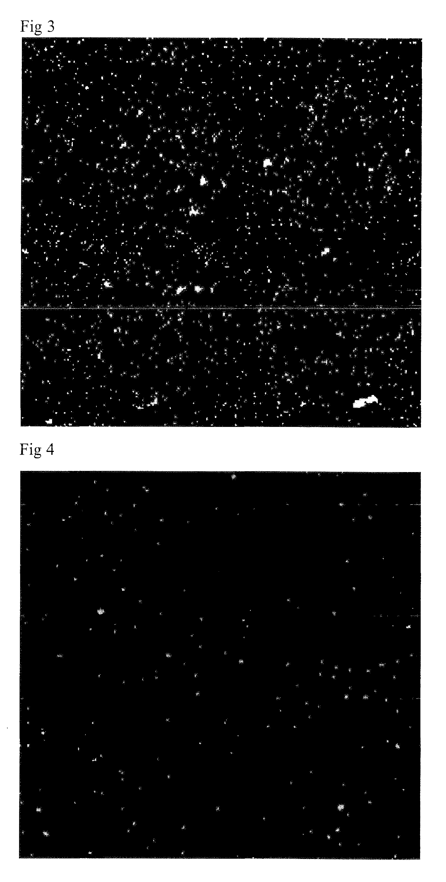
Image

Examples
example 1
[0064]In Example 1, the foregoing In2O3 powder (1) having a grain size of 10.7 μm and a specific surface area of 4.4 m2 / g was used as the In2O3 raw material, the foregoing Ga2O3 powder (2) having a grain size of 4.6 μm and a specific surface area 11.9 m2 / g was used as the Ga2O3 raw material, and the foregoing ZnO powder (1) having a grain size of 1.07 μm and a specific surface area of 3.8 m2 / g was used as the ZnO raw material. The raw materials were mixed so that these powders will be at a molar ratio of In2O3:Ga2O3:ZnO=1:1:1.
[0065]Subsequently, these powders were mixed, and additionally calcinated in the atmosphere at 950° C. for 5 hours. The specific surface area (BET) before and after pulverization was 3.1 m2 / g and 14.7 m2 / g, respectively. Thus, the difference was 11.6 m2 / g.
[0066]The foregoing results are collectively shown in Table 3. The powder mixing, pulverization, calcination, sintering, and target production were conducted based on the conditions shown in foregoing paragrap...
example 2
[0071]In Example 2, the foregoing In2O3 powder (1) having a grain size of 10.7 μm and a specific surface area of 4.4 m2 / g was used as the In2O3 raw material, the foregoing Ga2O3 powder (1) having a grain size of 5.6 μm and a specific surface area of 9.1 m2 / g was used as the Ga2O3 raw material, and the foregoing ZnO powder (1) having a grain size of 1.07 μm and a specific surface area of 3.8 m2 / g was used as the ZnO raw material. The raw materials were mixed so that these powders will be at a molar ratio of In2O3:Ga2O3:ZnO=1:1:1.
[0072]Subsequently, these powders were mixed, and additionally calcinated in the atmosphere at 950° C. for 5 hours. The specific surface area (BET) before and after pulverization was 2.6 m2 / g and 17.0 m2 / g, respectively. Thus, the difference was 14.4 m2 / g.
[0073]The results are collectively shown in Table 3. The same methods as Example 1 were conducted as to the powder mixing, pulverization, calcination, sintering and target production, and various measurement...
example 3
[0076]In Example 3, the foregoing In2O3 powder (3) having a grain size of 1.6 μm and a specific surface area of 5.8 m2 / g was used as the In2O3 raw material, the foregoing Ga2O3 powder (2) having a grain size of 5.6 μm and a specific surface area 9.1 m2 / g was used as the Ga2O3 raw material, and the foregoing ZnO powder (1) having a grain size of 1.07 μm and a specific surface area 3.8 m2 / g was used as the ZnO raw material. The raw materials were mixed so that these powders will be at a molar ratio of In2O3:Ga2O3:ZnO=1:1:1.
[0077]Subsequently, these powders were mixed, and additionally calcinated in the atmosphere at 1350° C. for 5 hours. The specific surface area (BET) before and after pulverization was 6.9 m2 / g and 17.1 m2 / g, respectively. Thus, the difference was 10.2 m2 / g.
[0078]The results are collectively shown in Table 3. The same methods as Example 1 were conducted as to the powder mixing, pulverization, calcination, sintering and target production, and various measurements and ...
PUM
| Property | Measurement | Unit |
|---|---|---|
| density | aaaaa | aaaaa |
| grain size | aaaaa | aaaaa |
| grain size | aaaaa | aaaaa |
Abstract
Description
Claims
Application Information