Method for repairing display device and apparatus for same

a display device and a technology for the same, applied in the field of repair methods of display devices and apparatuses for the same, can solve the problems of short-circuiting and disconnection of wires, inferior products, uneven color, etc., and achieve the effects of preventing defects, uniform surface quality, and reducing inconsistency in the quality of formed films

Active Publication Date: 2015-06-23
PANASONIC LIQUID CRYSTAL DISPLAY CO LTD +1
View PDF20 Cites 0 Cited by
  • Summary
  • Abstract
  • Description
  • Claims
  • Application Information

AI Technical Summary

Benefits of technology

[0033]According to the present invention, a wide variety of regions can be repaired in various ways using various materials. In addition, inconsistency in the quality of the formed film can be reduced, the surface quality can be uniformly improved, and defects can be prevented, and thus, the cost of manufacture can be lowered.

Problems solved by technology

When there is a defect in the pattern of the color filter or a wire, the display of the liquid crystal display device becomes abnormal, and thus the product is inferior.
Display abnormalities include color defects caused by the resin applied on the color filter sticking out over an adjoining pixel, unevenness in the color caused by inconsistency in the film thickness of the resins or the TFT substrate, short-circuiting and disconnection of wires and the like.
When there is a defect on the circuit or the color filter, the liquid crystal display element has abnormal display, and thus becomes a defective product.
Therefore, when the substrate is entirely surrounded by a chamber, the apparatus becomes very large, and problems arise, such that it takes time to replace the air within the chamber with an inert gas, such as argon, and in addition, the cost of the inert gas is high.

Method used


Image

  • Method for repairing display device and apparatus for same
  • Method for repairing display device and apparatus for same
  • Method for repairing display device and apparatus for same

Examples


first embodiment

[0066](First Embodiment)

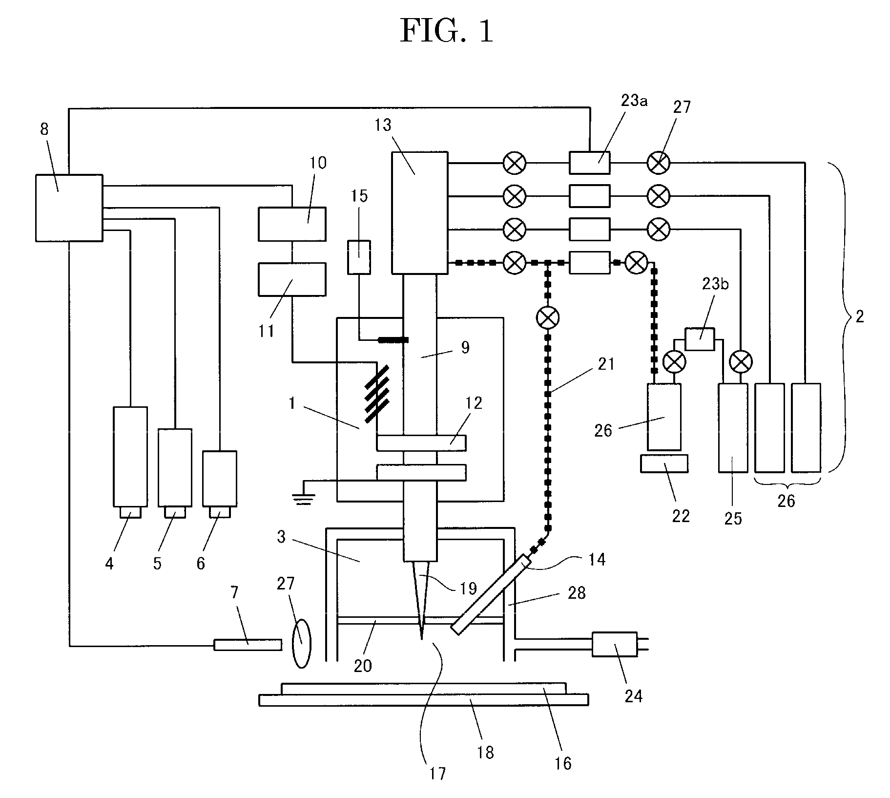
[0067]FIG. 1 is a schematic diagram showing the apparatus for repairing a liquid crystal display device (which may hereinafter sometimes be referred to as repairing apparatus) according to the first embodiment of the present invention.

[0068]The repairing apparatus in FIG. 1 is, roughly, formed of a local plasma generating portion 1 for repairing a defect, a gas supplying portion 2, a plasma reaction portion 3, a laser 4 for microscopic processing, an application mechanism 5, a camera 6 for detecting a defect, a measuring mechanism 7 for monitoring the condition of the plasma, and a control portion 8.

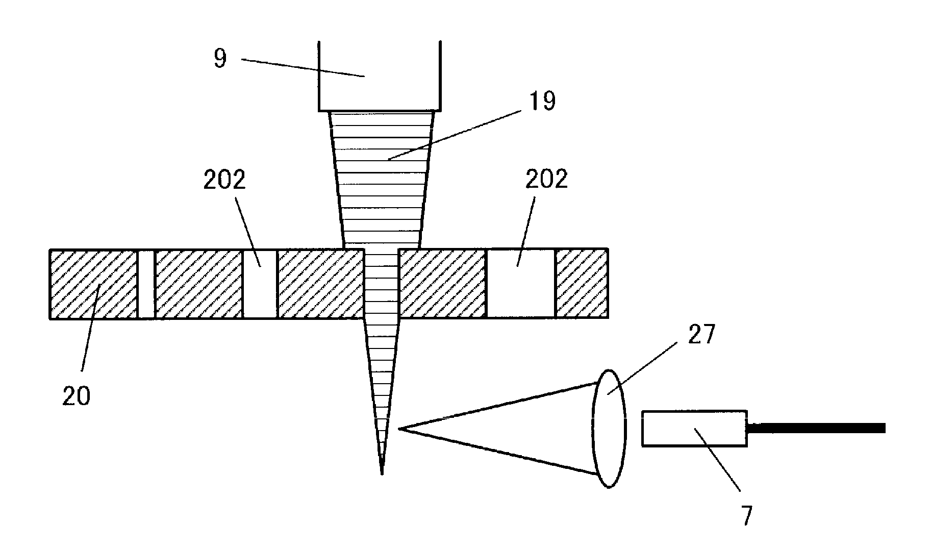
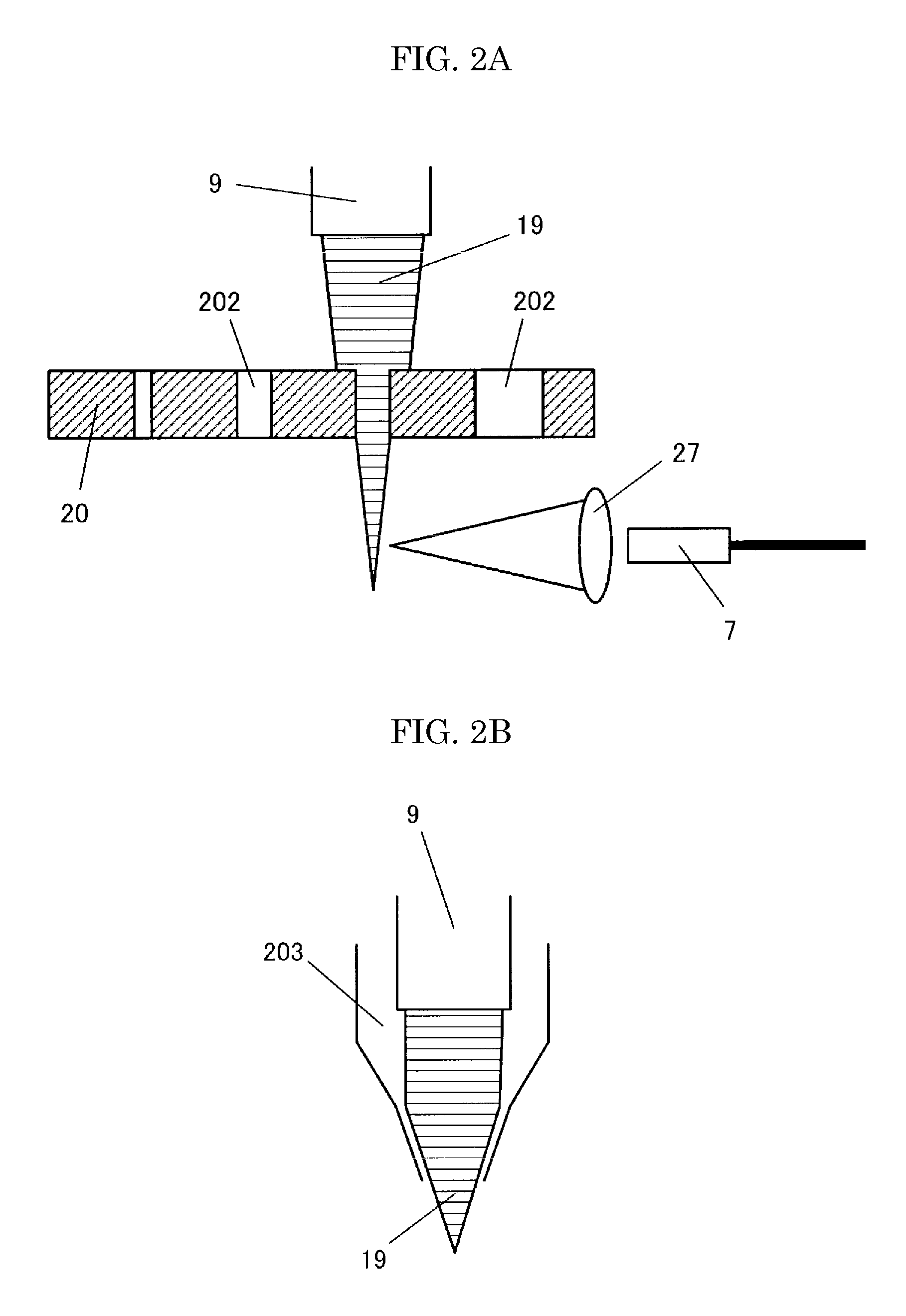
[0069]The plasma generating portion 1 is formed of a tubule 9 for generating plasma made of a dielectric body, such as of crystal, and an electrode 12 provided in the outer peripheral region of this tubule 9 which supplies high-frequency power from a high-frequency power supply 10 via a matching network 11. As a concrete example, a crystal tube having an inner dia...

second embodiment

[0098](Second Embodiment)

[0099]Next, the method for repairing a defect in a liquid crystal display device using the above described repairing apparatus according to the second embodiment of the present invention is described.

[0100]Here, the configuration of the liquid crystal display device where a defect is to be repaired is briefly described in reference to FIGS. 3A and 3B prior to the description of the method for repairing a defect. FIG. 3A is a cross sectional diagram and FIG. 3B a plan diagram showing a pixel portion.

[0101]In the configuration shown in FIG. 3A, a TFT substrate 311 where a number of pixel portions are formed and a filter substrate 312 where a number of color filters 308 are formed are provided in such a manner that the pixel portions and the color filters 308 face each other and liquid crystal 310 is sandwiched in between. In addition, as shown in FIG. 3B, gate wires 305 are formed in the above described pixel portions on the TFT substrate 311, and a gate insul...

third embodiment

[0133](Third Embodiment)

[0134]The third embodiment of the present invention relates to a process for repairing a defective portion using the same repairing apparatus as that above and a laser processing apparatus having an application mechanism for applying a resin based material, for example a resin for a contact mask, and a mechanism for microscopic processing of several μm, and irradiating a wide area of several hundred μm with a laser.

[0135]In the above described plasma jet 19, the intensity of plasma with which the substrate 16 is irradiated has a Gaussian distribution. Therefore, it is difficult to carry out a microscopic process in the micrometers with high precision, due to the distribution of the properties relating to the film thickness and the film quality from the center portion to the peripheral portion of the region irradiated with plasma. Thus, a mask process using a resin based material is used in the present embodiment.

[0136]FIG. 6 shows a procedure for repairing a ...


PUM

PropertyMeasurementUnit
lengthaaaaaaaaaa
outer diameteraaaaaaaaaa

Abstract

An object of the present invention is to provide a method for repairing a display device according to which a wide variety of regions can be repaired in various ways using various materials, as well as an apparatus for the same. The present invention provides a repairing apparatus for repairing a pattern defect on a surface of a substrate in a display device where an electronic circuit pattern having the above described pattern defect is formed, characterized by having a plasma irradiation means for repairing the above described pattern defect through local irradiation of a region including the above described pattern defect with plasma.

Description

[0001]The present application claims priority over Japanese Application JP2008-227750 filed on Sep. 5, 2008 and Japanese Application JP 2008-247112 filed on Sep. 26, 2008, the contents of which are hereby incorporated into this application by reference.BACKGROUND OF THE INVENTION[0002](1) Field of the Invention[0003]The present invention relates to a method for repairing a display device and an apparatus for the same, and in particular, to a technology for repairing a display device using a plasma jet generated under atmospheric pressure so that a short-circuited portion or an open portion of the electrical circuit pattern on the substrate becomes normal.[0004]In addition, the present invention also relates to a manufacturing method according to which a film can be locally formed or a surface locally processed, as well as a manufacturing apparatus for the same, and in particular, to a technology for local film formation or surface processing with a gas flowing through a reaction cha...

Claims


Application Information

Patent Timeline
Patent Type & Authority Patents(United States)
IPC IPC(8): C23C16/44C23C16/52C23C16/00G02F1/13
CPCG02F1/1309
Inventor ARAI, TAKESHINAKASU, NOBUAKIEDAMURA, TADAOOROKU, NORIYUKI
Owner PANASONIC LIQUID CRYSTAL DISPLAY CO LTD
Why Eureka
Try Eureka