Embedded arrays of vertically aligned carbon nanotube carpets and methods for making them
a technology of carbon nanotubes and carpets, applied in the direction of carbon-silicon compound conductors, nanoinformatics, transportation and packaging, etc., can solve the problems of low variety of substrates suitable for growth and inability to be conductive, and achieve the effect of superior mechanical
- Summary
- Abstract
- Description
- Claims
- Application Information
AI Technical Summary
Benefits of technology
Problems solved by technology
Method used
Image
Examples
example 1
[0055]This example illustrates providing an entangled carbon nanotube mat integral with a carbon nanotube array by using carbon nanotube carpet growth. This method was used to prepared the carpets, and thus the entangled mats, used in Examples 2 and 3.
[0056]VA-SWNT films were grown according to Hata et al.'s report (Hata, K.; Futaba, D. N.; Mizuno, K.; Namai, T.; Yumura, M.; Iijima, S. Science 2004, 306, 1362-1364). For the catalyst preparation, 10 nm of Al2O3 was deposited using e-beam evaporator onto a Si-substrate with 3.5 μm silicon oxide layer, and additionally 1 nm Fe was deposited as a catalyst. The growth condition was ethylene: H2: Ar=100 sccm: 400 sccm: 600 sccm at 750° C. at 1 atm total pressure for 10 min.
[0057]The first few experiments were tried with and without water, but no vertically aligned film was grown in the absence of catalyst pretreatment. Later, the present inventors found that the pretreatment of deposited catalysts tends to be imperative. Oxidation at 500°...
example 2
[0061]This example illustrates a system and method involving embedding an entangled mat in an adhesive embedding material.
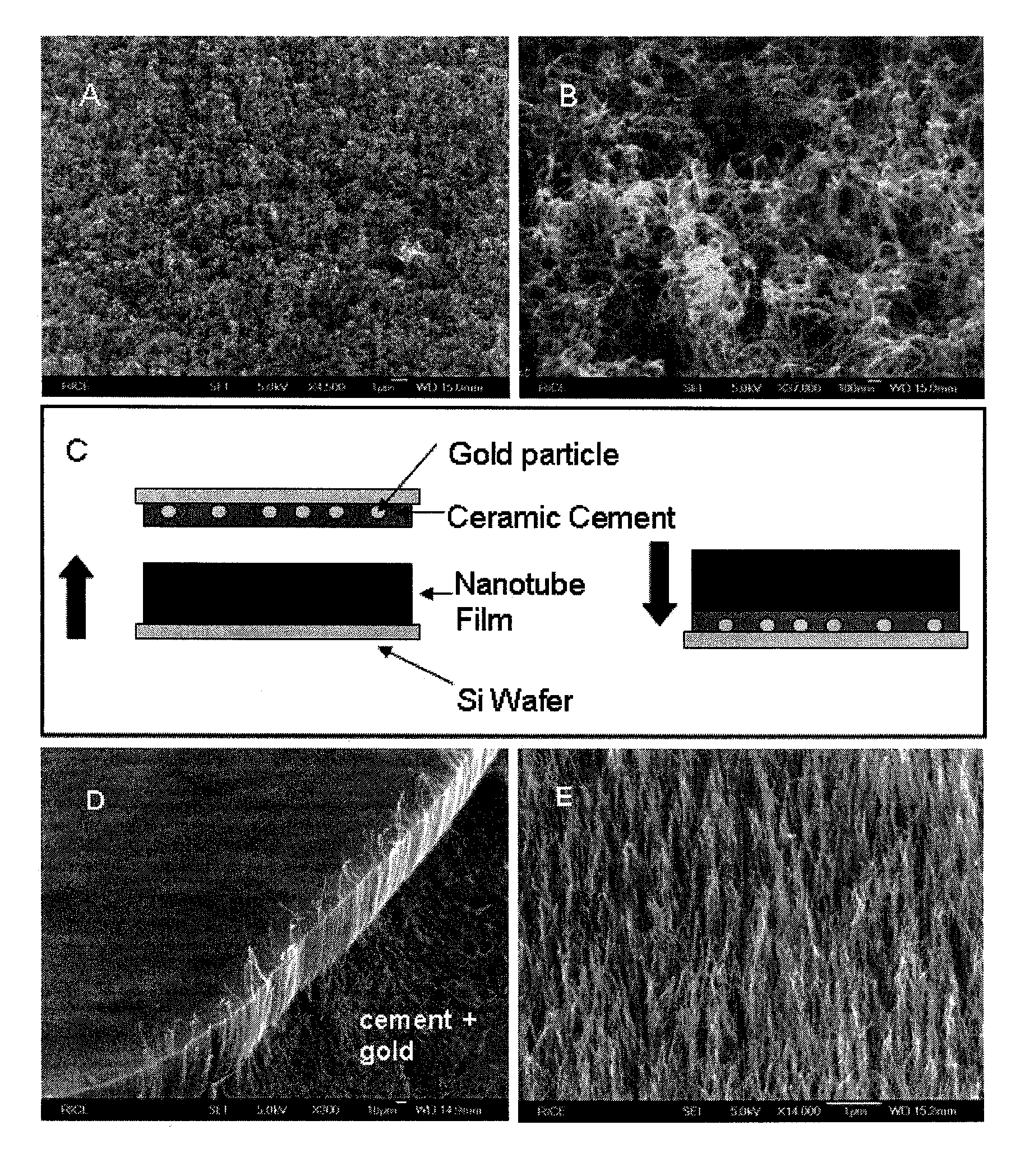
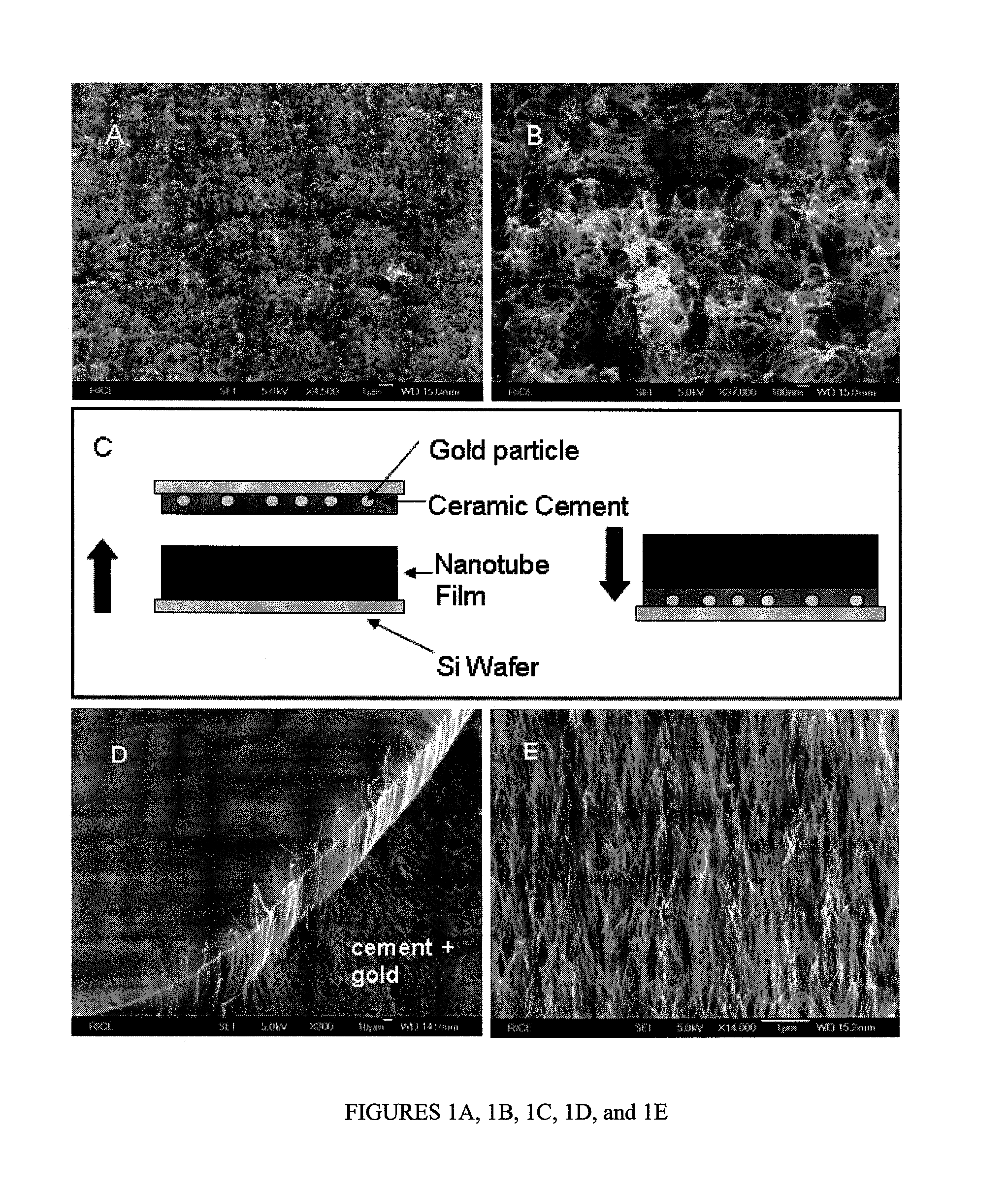
[0062]As shown in FIG. 1 (C), ceramic cement (Omega CC High Temperature cement) was mixed with liquid binder and spread uniformly on a silicon wafer. A VA-SWNT film was contacted to cement mixtures and cured for 24 hours at room temperature or 4 hours at 65° C. After curing, a VA-SWNT film was detached by a mechanical force applied between two substrates. Thus, an optically flat surface of exposed carbon nanotube bundle tips is created which is mechanically strong and resilient against high temperature exposures.
[0063]As illustrated in FIGS. 1 (D) and (E), the VA-SWNT film has been flipped over, exposing optically flat surface and very well aligned clean bundles. The whole thickness of the films transferred over due to high tensile strength of nanotubes. Gold particles can be embedded in cement in order to confer conductivity through the transfer base as indicate...
example 3
[0064]This example illustrates a system and method involving embedding an entangled mat in a depositable embedding material.
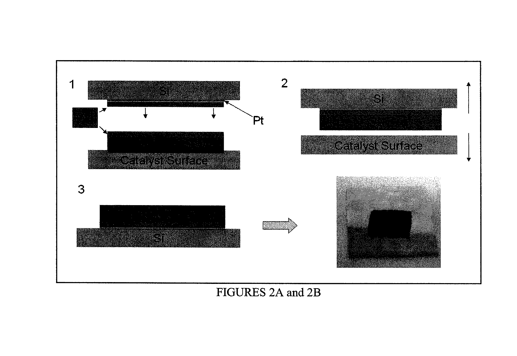
[0065]A 70 nm thick gold layer was deposited by a sputter coater or an e-beam evaporator onto both Si wafer coated in a thin Pt layer and VA-SWNT film. The gold-coated VA-SWNT film was pressed against the gold-coated Si wafer and baked in Ar at 800° C. for 5 minutes to fuse the two gold films. High pressure tends to produce a bending of the nanotubes in the carpet which is retained as a wavy morphology. Such bending also creates a shearing force between the nanotube and the substrates in contact. the transfer substrate is thought to have a higher resistance to shear force so that the nanotube is preferentially debonded from the growth substrate. After baking, the Si wafer and growth substrate were pried apart; the flipped-over film was removed from the growth surface and transferred intact to the transfer substrate. Through this means, we were able to flip over...
PUM
| Property | Measurement | Unit |
|---|---|---|
| thick | aaaaa | aaaaa |
| pressure | aaaaa | aaaaa |
| diameter | aaaaa | aaaaa |
Abstract
Description
Claims
Application Information
 - R&D Engineer
- R&D Manager
- IP Professional
- Industry Leading Data Capabilities
- Powerful AI technology
- Patent DNA Extraction
Browse by: Latest US Patents, China's latest patents, Technical Efficacy Thesaurus, Application Domain, Technology Topic, Popular Technical Reports.
© 2024 PatSnap. All rights reserved.Legal|Privacy policy|Modern Slavery Act Transparency Statement|Sitemap|About US| Contact US: help@patsnap.com


