Data sampling devices
a data sampling and data technology, applied in the field of semiconductor integrated circuits, can solve the problems of signal delay, mishandling of sampling, and reducing the reliability of the sampling device of the memory, and achieve the effect of tolerable delay bound of signals
- Summary
- Abstract
- Description
- Claims
- Application Information
AI Technical Summary
Benefits of technology
Problems solved by technology
Method used
Image
Examples
first embodiment
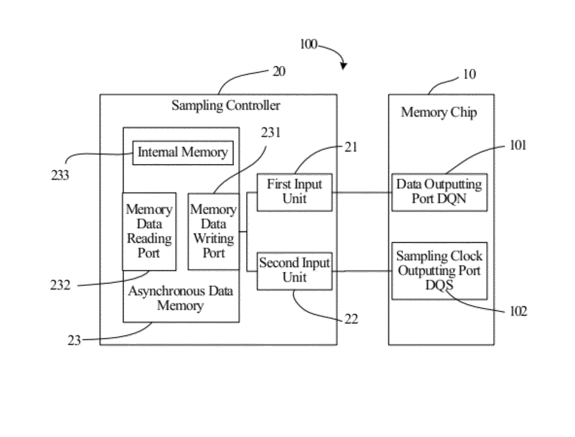
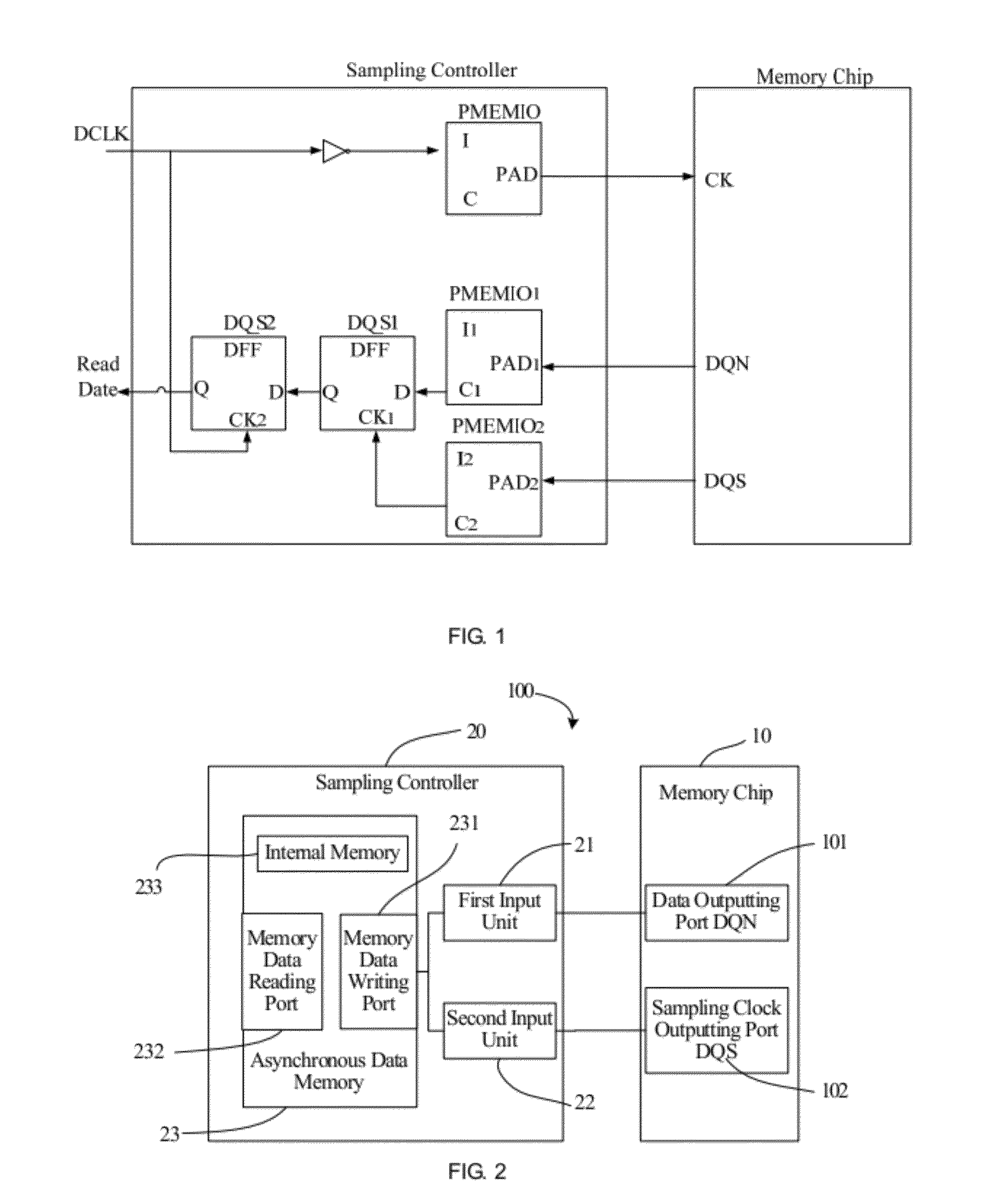
[0024]Referring now to FIG. 2, it shows an exemplary data sampling device 100 according to a The device 100 includes a memory chip 10 and a sampling controller 20. The memory chip 10 includes a data output port DQN 101 for output sampling data from the memory chip 10 and a sampling clock output port DQS 102 for output a sampling clock signal. The sampling controller 20 includes a first input unit 21 for receiving the sampling data from the data output port DQN 101, and a second input unit 22 for receiving the clock signal from the sampling clock output port DQS 102, and an asynchronous data memory 23. The asynchronous data memory 23 includes a memory data writing port 231, a memory data reading port 232, and an internal memory 233. The memory data writing port 231 receives the clock signal, employs the clock signal as its writing clock signal, and stores the sampling data of the first input unit 21 into the internal memory 233 according to the writing clock signal. The memory data ...
second embodiment
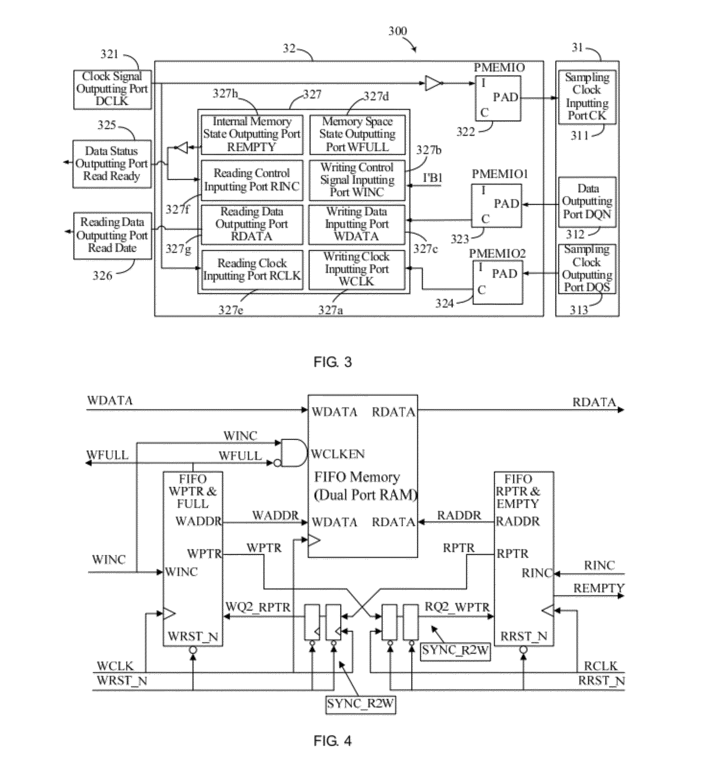
[0028]Referring to FIG. 3, it is a DDR data sampling device 300 according to the present invention. The DDR data sampling device 300 uses a DDR SDRAM (Double Date Rate Synchronous Dynamic Random Access Memory). The DDR data sampling device 300 includes a DDR chip 31 and a DDR controller 32.
[0029]The DDR chip 31 includes a sampling clock input port CK 311, a data output port DQN 312, and a sampling clock output port DQS 313. The sampling clock input port CK 311 is configured for receiving a clock, which is used as a working clock of the DDR chip 31, from outside of the DDR chip 31. The data output port DQN 312 is configured for output the sampling data in the DDR chip 31. The sampling clock output port DQS 313 is configured for output a sampling clock signal of the DDR chip 31.
[0030]The DDR controller 32 includes a clock signal input port DCLK 321, a clock signal output unit PMEMIO 322, a first input unit PMEMIO1323, a second input unit PMEMIO2324, a data status output port Read Read...
PUM
 Abstract
Description
Claims
Application Information


