Double mirror structure for wavelength division multiplexing with polymer waveguides

a polymer waveguide and wavelength division technology, applied in optical waveguide light guides, instruments, optics, etc., can solve the problems of increasing the total increasing the bandwidth of the system, and increasing the density of the physical limi

Active Publication Date: 2015-07-21
GLOBALFOUNDRIES US INC
View PDF13 Cites 23 Cited by
  • Summary
  • Abstract
  • Description
  • Claims
  • Application Information

AI Technical Summary

Problems solved by technology

However, despite these developments, new multi-core processing architectures demand higher bandwidth and density.
In the most advanced systems, more than 60,000 individual fibers are used, so that practical physical limits are being rapidly reached.
This increases the total bandwidth of a system without a corresponding increase in the number of physical channels, but existing wavelength division multiplexing solutions are difficult to implement on optical printed circuit board technology.
However, it is difficult to form such a reflector on a polymer waveguide, it is difficult to form structures on a forty-five degree angle due to shadow effects, and the reflector itself must be relatively thick due to a large polarization dependency that results from the forty-five degree angle of incidence.

Method used


Image

  • Double mirror structure for wavelength division multiplexing with polymer waveguides
  • Double mirror structure for wavelength division multiplexing with polymer waveguides
  • Double mirror structure for wavelength division multiplexing with polymer waveguides

Examples


Embodiment Construction

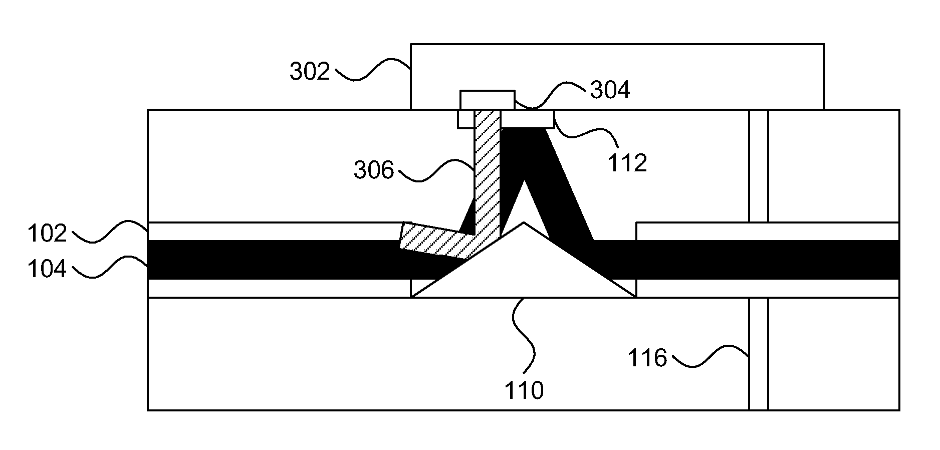
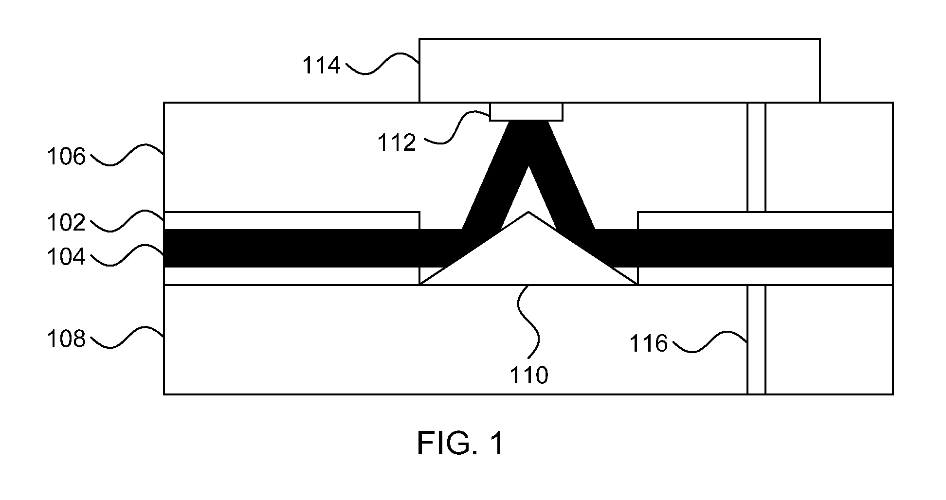
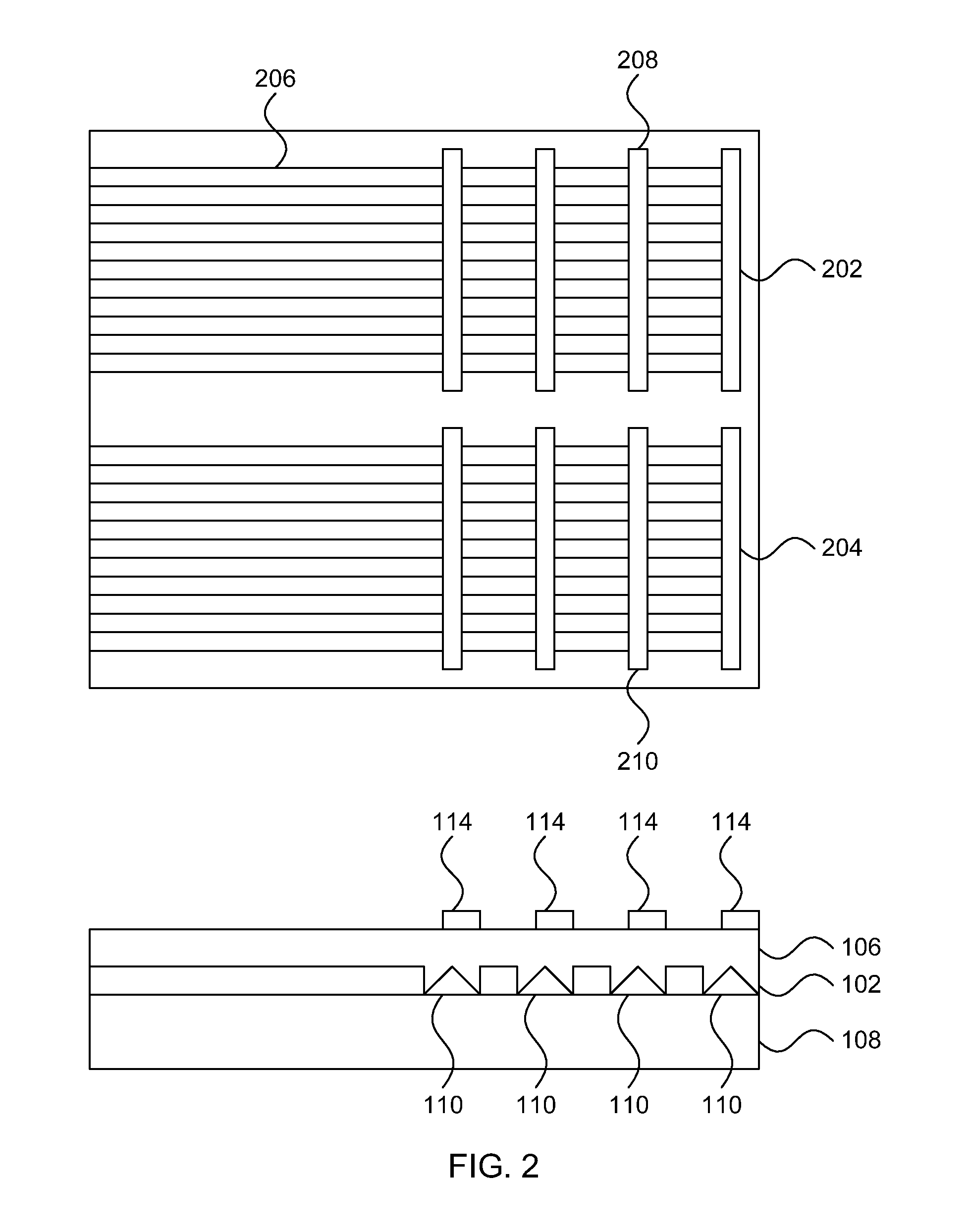
[0025]Embodiments of the present invention provide wavelength division multiplexing (WDM) in a polymer waveguide structure having an array of cores with a high density. The present embodiments use a double mirror structure with a dielectric filter deposited on an opto-electronic device array or on the top cladding to form wavelength filters. Although it is specifically contemplated that polymer waveguides be used in the present embodiments, it should be recognized that the present principles may be readily extended to other types of waveguide. Polymer waveguides and micromirrors guide the light from laser arrays with a high density, for example a 125 um core pitch. The signals from a board can be sent directly to another board via polymer waveguides for short range integrated data transfer, or can be coupled to a fiber ribbon for longer range data transfer.

[0026]Referring now to the drawings in which like numerals represent the same or similar elements and initially to FIG. 1, a WDM...


PUM

PropertyMeasurementUnit
angleaaaaaaaaaa
angle of incidenceaaaaaaaaaa

Abstract

Methods for wavelength filtering and structures for accomplishing the same. Wavelength filtering includes forming grooves in a waveguide to define angled surfaces in a path of the waveguide; forming a reflective layer on the angled surfaces; depositing cladding material on top of the waveguide and on the angled surfaces; forming a filter layer on an active region of an opto-electronic device, which transmits a single wavelength and reflects other wavelengths used; depositing the opto-electrical device on the cladding layer such that the filter layer is aligned with a point of incidence of a light beam reflected from the reflective layer; and electrically bonding the opto-electronic device to vias in the waveguide structure.

Description

BACKGROUND[0001]1. Technical Field[0002]The present invention relates to fiber optics systems and, more particularly, to wavelength division multiplexing with polymer waveguides.[0003]2. Description of the Related Art[0004]Optical data transfer is increasingly used in high-performance computing, where short-range optical communication provides a fast and low power alternative to electrical communication. However, despite these developments, new multi-core processing architectures demand higher bandwidth and density. The number of channels needed to transfer information is increasing rapidly. In the most advanced systems, more than 60,000 individual fibers are used, so that practical physical limits are being rapidly reached.[0005]Efforts have been made to use a single fiber to carry multiple data signals at different wavelengths. This increases the total bandwidth of a system without a corresponding increase in the number of physical channels, but existing wavelength division multip...

Claims


Application Information

Patent Timeline
Patent Type & Authority Patents(United States)
IPC IPC(8): G02B6/12G02B6/42
CPCG02B6/4215G02B6/4214G02B6/12007G02B6/132G02B2006/12109G02B2006/12164Y10T29/49117
Inventor HEROUX, JEAN BENOIT
Owner GLOBALFOUNDRIES US INC
Why Eureka
Try Eureka