Non-volatile static ram cell circuit and timing method

a non-volatile static, ram cell technology, applied in the direction of digital storage, line/current collector details, instruments, etc., can solve the problems of insufficient current to carry out a write “0” operation, loss of data, and inability to provide enough current to carry out a write “1” operation

Active Publication Date: 2015-08-04
SAMSUNG SEMICON
View PDF21 Cites 9 Cited by
  • Summary
  • Abstract
  • Description
  • Claims
  • Application Information

AI Technical Summary

Problems solved by technology

Therefore, where loss of data due to power failure or termination is unacceptable, a non-volatile memory is used to store the data.
Accordingly, a write driver circuit adapted to deliver sufficient current to write a “0”, may not be able to provide enough current to write a “1”.
Accordingly, the voltages designed to generate the critical current needed to carry out a write “0” operation may not be sufficient to carry out a write “1” operation.
An undesirable asymmetry thus exists in the current levels during write “1” and write “0” operations.
Consequently, a transistor size selected to provide sufficient current to write a “0” may not provide enough current to write a “1”.
Alternatively, a larger transistor size selected to provide the required current to write a “1”, may result in generation of excessive current when writing a “0”.

Method used


Image

  • Non-volatile static ram cell circuit and timing method
  • Non-volatile static ram cell circuit and timing method
  • Non-volatile static ram cell circuit and timing method

Examples


Embodiment Construction

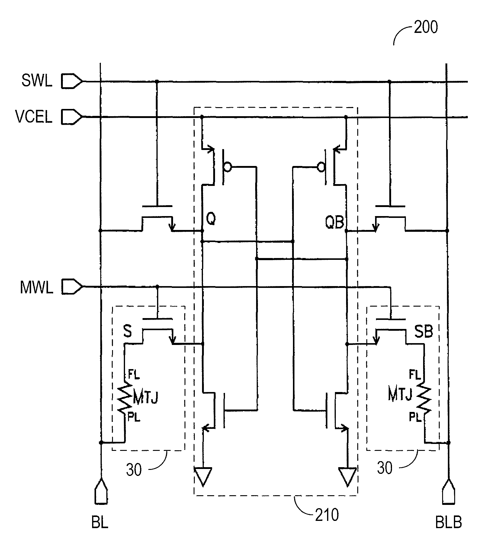
[0062]In accordance with embodiments of the present invention, data stored in a volatile SRAM memory may also be stored in separate non-volatile memory (NVM) circuits. During system power up, data from the NVM may be loaded into SRAM where system operations are executed faster. When power is shut down it may be desirable to transfer data currently in SRAM to NVM so the latest data can be available again after power is restored. When the NVM and SRAM are implemented on separate chips in a system, the speed of data transfer is limited by the relatively long time and high power taken to drive large capacitive and or inductive interconnect circuit loads between the chips. In addition, the data transfer speed is limited by the narrow data bus width between chips. These limitations can be reduced by integrating the SRAM and NVM on the same SOC. But separate memory circuits may still require separate dedicated ancillary circuits such as decoders, sense amplifiers and control circuits which...


PUM

PropertyMeasurementUnit
Vpp programming voltageaaaaaaaaaa
voltagesaaaaaaaaaa
voltagesaaaaaaaaaa

Abstract

A non-volatile static random access memory cell and includes a bistable regenerative circuit coupled to first and second transistors and to first and second non-volatile memory cells. Methods of use include directly transferring a complementary data bit between the non-volatile memory cell and the bistable regenerative circuit. Alternatively, complementary data from the bistable regenerative circuit may be regenerated by a sense amplifier and a second bistable regenerative circuit before being transferred to non-volatile memory cells in a column of memory cells. The bistable regenerative circuit may be reset to ground potential. Applications using the non-volatile SRAM cell with direct read out from the bistable regenerative circuit include a non-volatile flip-flop or non-volatile multiplexer.

Description

CROSS-REFERENCES TO RELATED APPLICATIONS[0001]The present application claims benefit under 35 USC 119(e) of U.S. provisional application No. 61 / 363,576, filed Jul. 12, 2010, entitled “Non-Volatile Static Ram Cell Circuit and Timing Method,” the content of which is incorporated herein by reference in its entirety.[0002]This application is related to commonly assigned application Ser. No. 61 / 352,306, filed Jun. 7, 2010, entitled “MULTI-SUPPLY SYMMETRIC DRIVER CIRCUIT AND TIMING METHOD”; commonly assigned application Ser. No. 12 / 558,451, filed Sep. 11, 2009, entitled “DIFFERENTIAL READ AND WRITE ARCHITECTURE”; and commonly assigned application Ser. No. 12 / 544,189, filed Aug. 19, 2009, entitled “DYNAMIC MULTISTATE MEMORY WRITE DRIVER,” the contents of all of which are incorporated herein by reference in their entirety.BACKGROUND OF THE INVENTION[0003]The present invention relates to memory integrated circuits, and more particularly to a non-volatile static random access memory.[0004]Sem...

Claims


Application Information

Patent Timeline
Patent Type & Authority Patents(United States)
IPC IPC(8): G11C14/00
CPCG11C14/0081G11C14/0072G11C14/009G11C14/0063Y10T29/49117
Inventor ONG, ADRIAN E.
Owner SAMSUNG SEMICON
Why Eureka
Try Eureka