

Semiconductor substrate and method for making the same
a semiconductor and substrate technology, applied in the field of substrates, can solve the problems of product failure, bump formation in the existing manner, and the inability to locate the bump right on the pads of the circuit layer, so as to achieve the effect of easy result and maintainable product yield
- Summary
- Abstract
- Description
- Claims
- Application Information
AI Technical Summary
Benefits of technology
Problems solved by technology
Method used
Image

Examples
Embodiment Construction
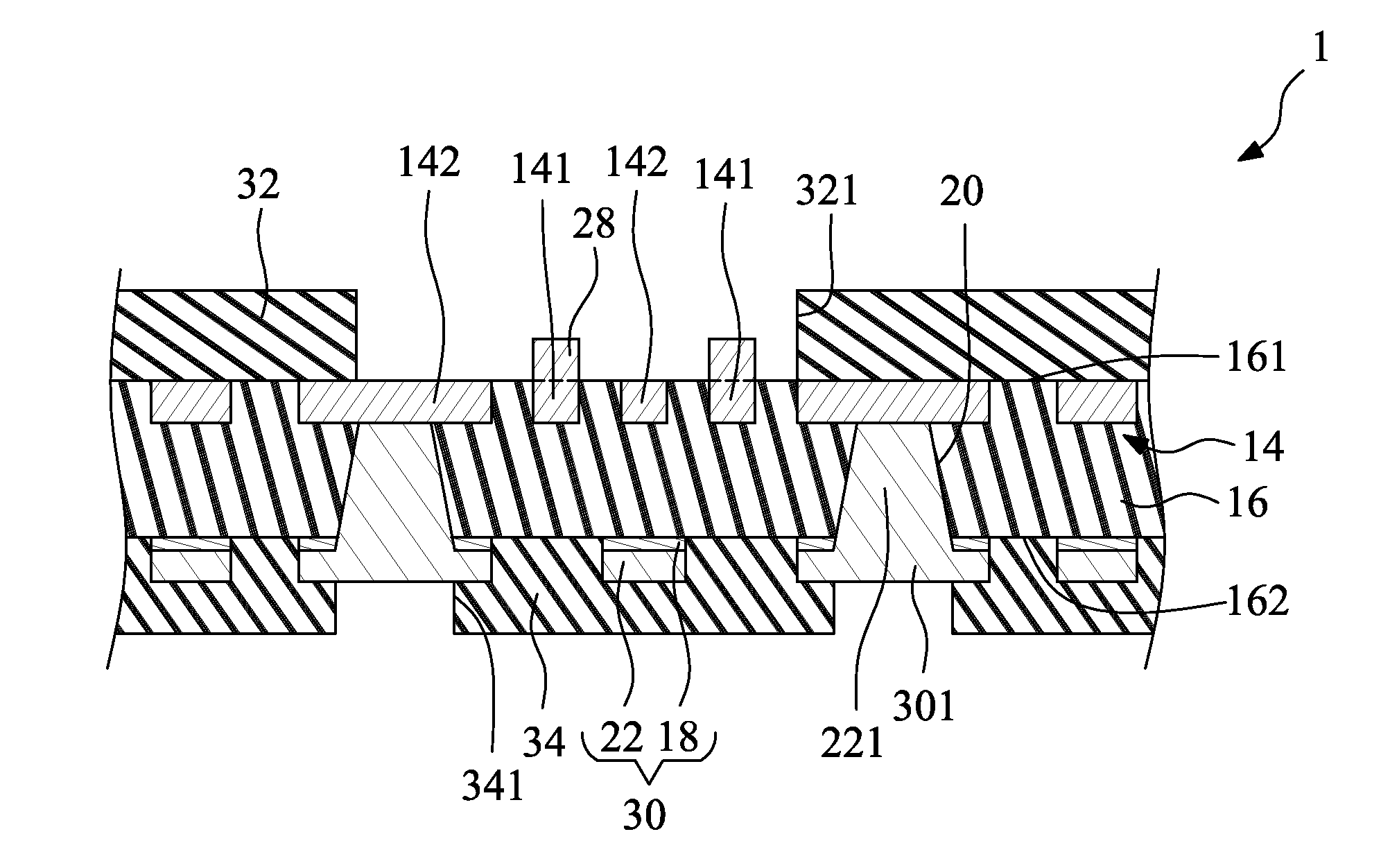
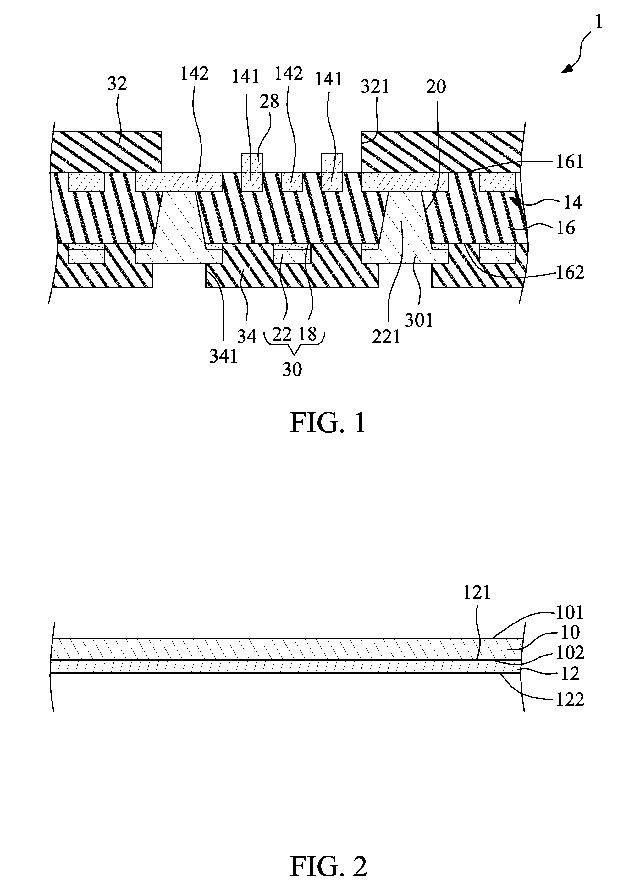
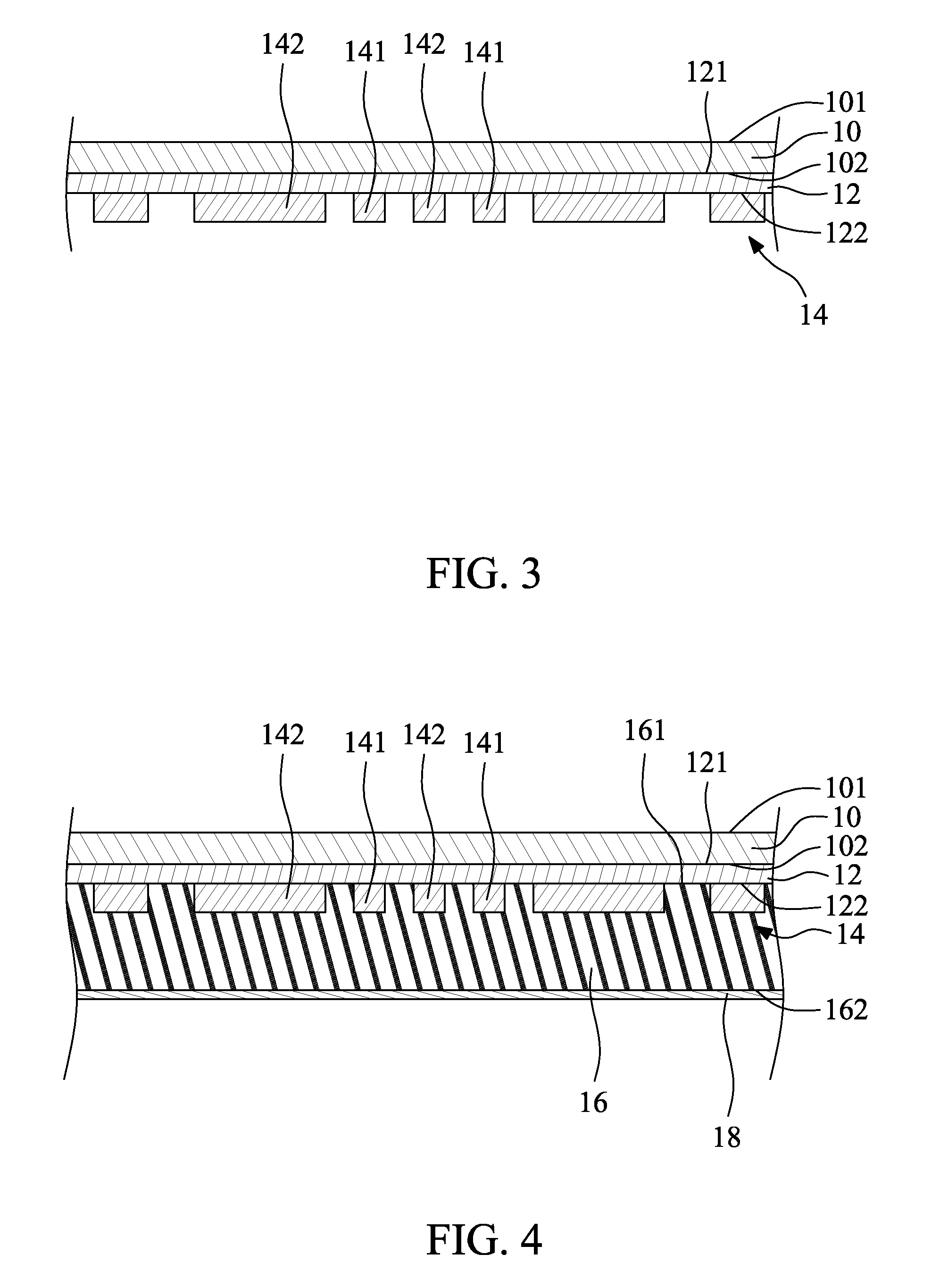
[0019]FIG. 1 is a schematic partial cross-sectional view of an embodiment of a semiconductor substrate according to the present disclosure. The semiconductor substrate 1 includes an insulation layer 16, a first circuit layer 14, a second circuit layer 30, a plurality of conductive vias 221, a plurality of bumps 28, a first protection layer 32 and a second protection layer 34.
[0020]The insulation layer 16 is made from an insulating material or a dielectric material, for example, Polypropylene (PP), which has a first surface 161, a second surface 162 and a plurality of through holes 20. The first circuit layer 14 is embedded in the first surface 161 of the insulation layer 16, and exposed from the first surface 161 of the insulation layer 16. An exposed surface of the first circuit layer 14 is substantially coplanar with the first surface 161 of the insulation layer 16. In this embodiment, the first circuit layer 14 is a patterned conductive circuit layer, including a plurality of pad...
PUM
 Abstract
Description
Claims
Application Information