Quantum dots (QD) for semiconductor integrated circuit

a semiconductor integrated circuit and quantum dots technology, applied in the field of quantum dots (qd) for semiconductor integrated circuits, can solve the problems of difficult detection and invisible to the unaided eye, and achieve the effect of good crystalline quality

Active Publication Date: 2015-08-25
HRL LAB
View PDF16 Cites 1 Cited by
  • Summary
  • Abstract
  • Description
  • Claims
  • Application Information

AI Technical Summary

Benefits of technology

[0015]self-assembled quantum dot constructs have good crystalline quality and a protective interface;
[0016]it is relatively simple as compared with other authentication or verification techniques;
[0019]because growth temperature of quantum dot structures is generally higher than known manner semiconductor process temperature, and because of three dimensional confinement (less temperature sensitivity), quantum dot structures are stable and are not expected to change with time;
[0021]in operation, identity authentication tests do not need any bias nor need to be triggered, no modification to response in detection is needed, and physical attacks can be sensed and verified.

Problems solved by technology

physical size of quantum dot structures make them invisible to the unaided-eye and difficult to detect even with the aid of systems such as scanning electron microscopes; and

Method used


Image

  • Quantum dots (QD) for semiconductor integrated circuit
  • Quantum dots (QD) for semiconductor integrated circuit
  • Quantum dots (QD) for semiconductor integrated circuit

Examples


Embodiment Construction

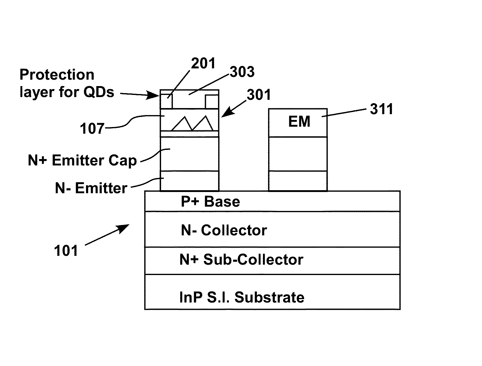
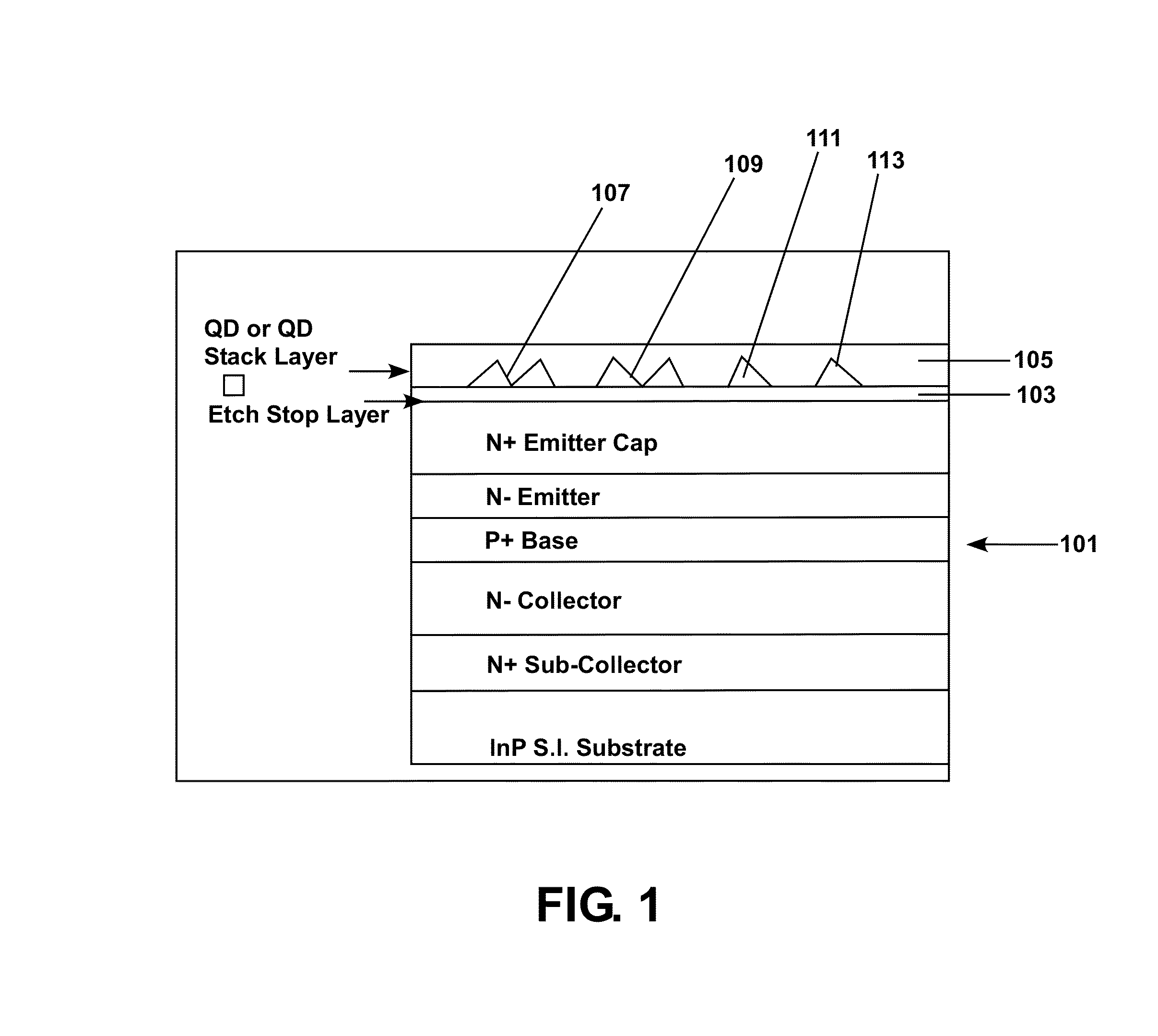
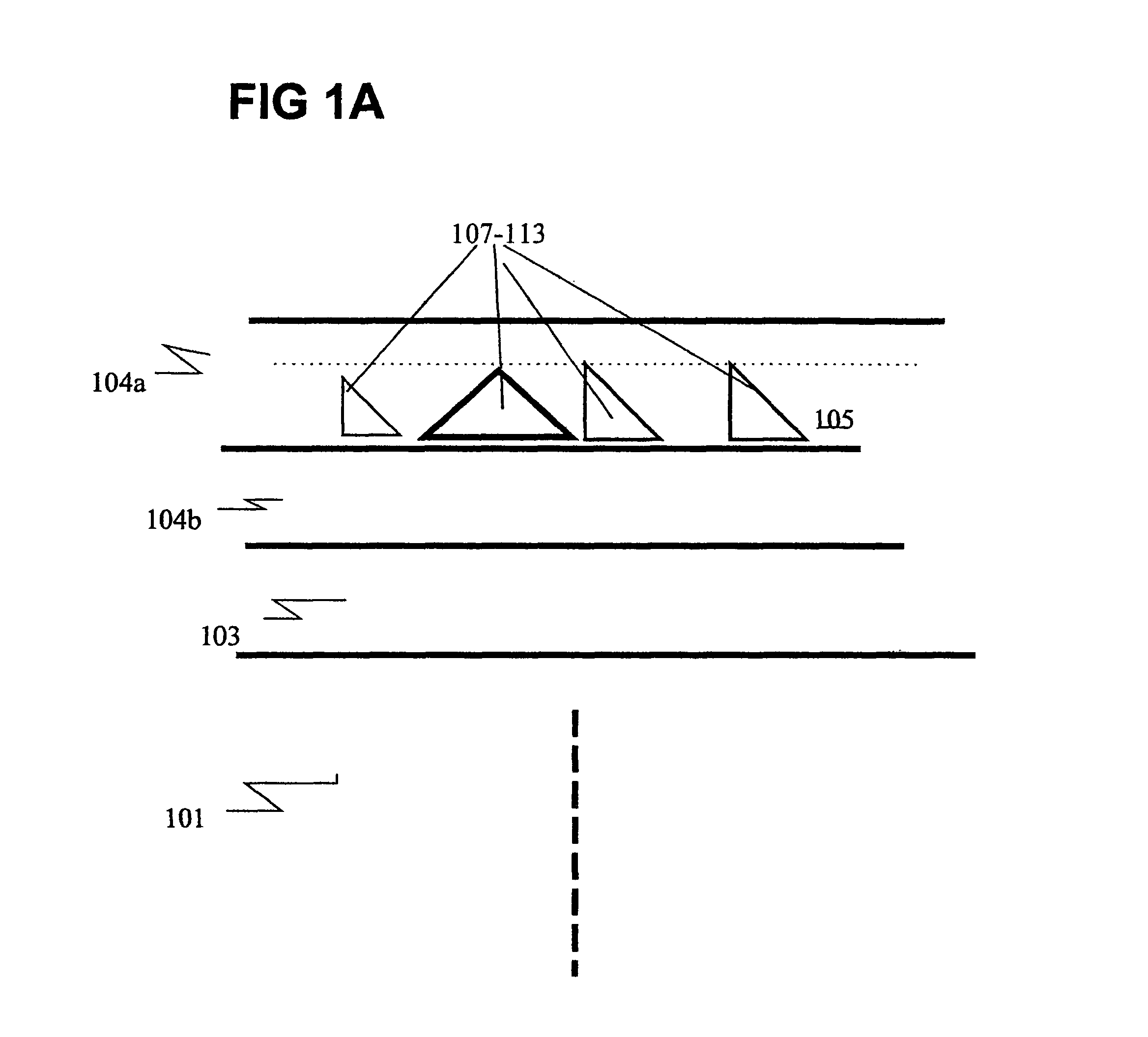
[0029]In general, the present invention provides for quantum dot target constructs that may be associated with semiconductor devices for the purpose of providing each of the devices with a unique, identifiable, code or set of codes. For convenience of explanation, the present invention is described in conjunction with the fabrication of an IC chip exemplary embodiment. However, it will be recognized by those skilled in the art that the invention may be practiced in conjunction with the fabrication of any semiconductor device in which the processes are compatible with the formation of quantum dot constructs. No limitation on the scope of the invention is intended by exemplary embodiment descriptions nor should any be implied therefrom. Standard periodic table symbols and integrated circuit symbols commonly understood by those skilled in the art are used throughout in the description.

[0030]FIG. 1 depicts a first stage of fabrication of a construct in accordance with the present invent...


PUM


Abstract

Semiconductor device identification using quantum dot technology. A semiconductor nanocrystal based target is fabricated. A guard ring superjacent the fluorescing surface of the nanocrystal surface is provided to ensure repeatability of spectral mapping and analysis data. A transparent cap on the target may enhance performance. A system for coding a semiconductor device is described. A method is described for fabricating quantum dot targets in a methodology compatible with subsequent semiconductor fabrication process steps.

Description

CROSS-REFERENCE TO RELATED APPLICATIONS[0001]This is a divisional application of U.S. patent application Ser. No. 11 / 542,814, filed on Oct. 3, 2006, which is incorporated herein as though set forth in full.STATEMENT REGARDING FEDERALLY SPONSORED RESEARCH OR DEVELOPMENT[0002]Not applicable.REFERENCE TO AN APPENDIX[0003]Not applicable.FIELD[0004]The technology described herein is generally related to the field of semiconductor devices and to the use of quantum dot technology to provide an integral, unique, reproducible identifier to be associated with each device.BACKGROUND[0005]A variety of technologies are used for semiconductor device identification, recognition, authentication, verification, security, and the like; for simplicity of explanation of the present invention, such issues and processes and mechanisms associated with such issues are generically referred to generically as “coding.” For example, to resolve such issues in semiconductor devices—e.g., integrated circuits (ICs)...

Claims


Application Information

Patent Timeline
Patent Type & Authority Patents(United States)
IPC IPC(8): G06F17/50H01L21/308
CPCH01L21/308G06F17/50H01L23/544H01L2223/54433H01L2223/54473H01L2223/5448H01L2924/0002H01L2924/00G06F30/00
Inventor CHEN, MARY Y.DEELMAN, PETER W.SOKOLICH, MARKO
Owner HRL LAB
Why Eureka
Try Eureka