Eureka AIR delivers breakthrough ideas for toughest innovation challenges, trusted by R&D personnel around the world.

Touch sensing electrode structure and method of manufacturing same

a technology electrode structures, which is applied in the direction of circuit optical details, non-metallic protective coating applications, instruments, etc., can solve the problems of low yield rate, inability to easily control the quality of metal conductive electrodes b>10/b>, and inability to form weatherproof layers in the second step, etc., to achieve stable control of the width of metal conductive electrodes, increase the service life of touch sensing electrodes, and increase the yield rate

Active Publication Date: 2015-09-08
APLUS SEMICON TECH CO LTD
View PDF1 Cites 7 Cited by
  • Summary
  • Abstract
  • Description
  • Claims
  • Application Information

AI Technical Summary

Benefits of technology

The present invention provides a method of manufacturing a touch sensing electrode structure that has a higher yield rate of metal conductive electrodes, increased service life, and reduced interference phenomenon of the moiré effect. The method includes using a masking layer with a predetermined circuit pattern to overcome the problem of low yield rate of metal conductive electrodes. The metal conductive electrodes are then covered by at least one weatherproof layer to protect against oxidation caused by moisture in the air. Additionally, the method allows for precise control of the width of each metal conductive electrode using the masking layer. The touch sensing electrode structure made by the method has increased light transmittance, reduced color cast, and increased comfort for viewing.

Problems solved by technology

Moreover, the weatherproof layer 13 formed in the second step usually has a non-uniform thickness.
Therefore, the metal conductive electrodes 10 are not easily controllable in quality and have low yield rate to form a tough problem in manufacturing very fine conductive electrodes.
Therefore, when the touchscreens using the metal conductive electrodes 10 manufactured with the conventional method have been used over a long time, their capacitive sensors might very possibly have a largely increased impedance value and could not operate in a normal state.

Method used


Image

  • Touch sensing electrode structure and method of manufacturing same
  • Touch sensing electrode structure and method of manufacturing same
  • Touch sensing electrode structure and method of manufacturing same

Examples


Embodiment Construction

[0054]The present invention will now be described with some preferred embodiments thereof and by referring to the accompanying drawings. For the purpose of easy to understand, elements that are the same in the preferred embodiments are denoted by the same reference numerals.

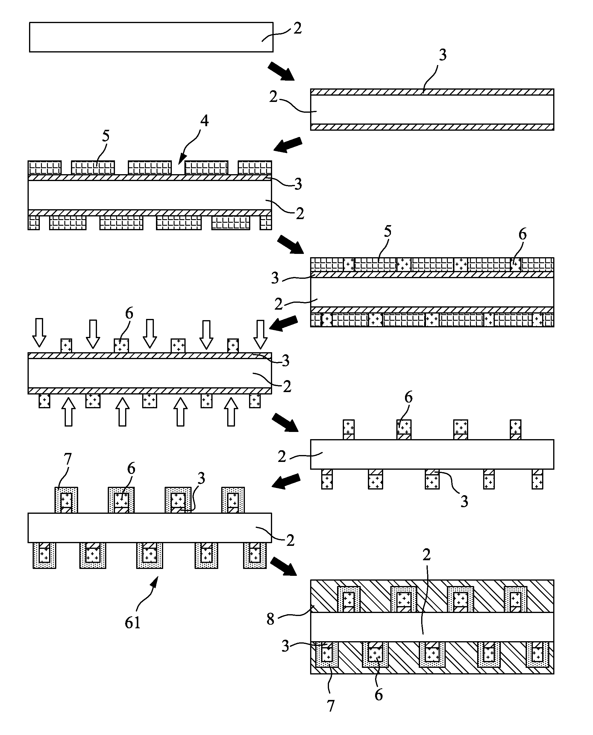
[0055]Please refer to FIG. 3A that is a flowchart showing the steps included in a first preferred embodiment of a method of manufacturing touch sensing electrode structure according to the present invention, and to FIG. 3B that is a pictorial description of the steps in the flowchart of FIG. 3A. The following is a detailed description of these steps, which are numbered from (A) to (F) herein for ease of reference.

[0056]Step (A): Select a predetermined substrate material and use the same to form a substrate layer 2. The substrate layer 2 can be formed of a soft material or a glass sheet. The soft material for forming the substrate layer 2 can be polyethylene terephthalate (PET), poly(methyl methacrylate) (PMMA), p...


PUM


Abstract

A method of manufacturing touch sensing electrode structure includes the steps of selecting a predetermined substrate material to form a substrate layer; forming at least one adhesion layer on the substrate layer; forming a masking layer with recessed lines on the adhesion layer; forming metal conductive electrodes in the recessed lines on the masking layer; removing the masking layer for the metal conductive electrodes to present a circuit pattern and etching off portions of the adhesion layer located between the metal conductive electrodes; and forming at least one weatherproof layer on peripheral surfaces of the metal conductive electrodes. The touch sensing electrode structure manufactured according to the above method has high yield rate and is weatherproof, and the metal conductive electrodes thereof have precisely controlled small width.

Description

FIELD OF THE INVENTION[0001]The present invention relates to a touch sensing electrode structure and a method of manufacturing same, and more particularly, to a touch sensing electrode structure manufacturing method, in which a masking layer is used in forming metal conductive electrodes for the touch sensing electrode structure and a weatherproof layer is formed to completely cover the metal conductive electrodes, so as to increase the yield rate of the touch sensing electrode structure and prolong the service life thereof.BACKGROUND OF THE INVENTION[0002]In response to the development of compact and light weight electronic information products, the semiconductor manufacturing process is now aimed to enable high-density and automated production. On the other hand, the currently available electronic information products are designed to have a touch sensing surface or touchscreen that is gradually increased in size. As a result, the conductive electrodes for the touchscreen originall...

Claims


Application Information

Patent Timeline
IPC IPC(8): G06F3/044G06F1/16G06F3/041
CPCG06F1/16G06F3/041G06F2203/04103G06F2203/04107G06F3/0445H05K1/0274H05K3/244H05K3/28H05K2201/0179
Inventor LAI, YU HAO
Owner APLUS SEMICON TECH CO LTD
Why Eureka
Eureka Blog
Learn More