Light emitting device, method of manufacturing light emitting device, and electronic equipment

a technology of light emitting devices and light emitting devices, which is applied in the direction of semiconductor devices, organic semiconductor devices, electrical equipment, etc., can solve the problems of color purity of light, emitted from light emitting areas, and difficult to enlarge the light emitting area over the boundary, so as to improve the color purity of blue, improve the effect of color purity and increase the light emitting area

Active Publication Date: 2015-09-22
SEIKO EPSON CORP
View PDF25 Cites 6 Cited by
  • Summary
  • Abstract
  • Description
  • Claims
  • Application Information

AI Technical Summary

Benefits of technology

[0014]Light, which is emitted from the light emission functional layer (light emission area), reciprocates between the light reflection layer and the facing electrode, and resonates according to an optical distance between the light reflection layer and the facing electrode, and thus light, which has a specific wavelength, is amplified. The optical distance varies according to the layer thicknesses of the first insulation layer. Since the first insulation layer includes three layer thicknesses, light of three types of resonant wavelengths is emitted. When the layer thicknesses of the first insulation layer are adjusted such that, for example, light of three types of resonant wavelengths, that is, blue, green, and red, is amplified, it is possible to enhance the color purity of the blue, green and red light which is emitted from the light emission area.
[0039]The first pixel electrode is formed in the first layer thickness part of the first insulation layer, the second pixel electrode is formed in the second layer thickness part of the first insulation layer, the third pixel electrode is formed in the third layer thickness part of the first insulation layer, each of the pixel electrodes is connected to the conductive layer, and the signal from the transistor is supplied through the conductive layer. Since the optical distance (the layer thicknesses of the first insulation layer) is fixed in the area in which each pixel electrode is formed, the variation in the resonant wavelength (deterioration of the color purity) is not generated even when the light emission area of the pixel electrode is enlarged. That is, compared to the well-known technique (JP-A-2009-134067) in which the area, in which the pixel electrode is provided, includes a boundary of different optical distance, it is possible to enlarge the light emission area without causing the color purity to be deteriorated and it is possible to enhance the intensity of light which is emitted from the light emission area. Accordingly, in the light emitting device according to the application example, it is possible to provide display with enhanced color purity and intensity of light, that is, display with brighter and clearer colors.

Problems solved by technology

In the electro-optic device disclosed in JP-A-2009-134067, if the light emission area is enlarged in order to acquire a brighter display, the boundary becomes an obstacle, and thus there is a problem in that it is difficult to enlarge the light emission area.
If the optical distance is different, the resonant wavelength varies, with the result that light of a different resonant wavelength is emitted from the light emission area, and thus the color purity of light, which is emitted from the light emission area, is deteriorated.
Therefore, there is a problem in that it is difficult to enlarge the light emission area over the boundary.

Method used


Image

  • Light emitting device, method of manufacturing light emitting device, and electronic equipment
  • Light emitting device, method of manufacturing light emitting device, and electronic equipment
  • Light emitting device, method of manufacturing light emitting device, and electronic equipment

Examples


first embodiment

Outline of Organic EL Apparatus

[0061]An organic EL apparatus 100 according to the first embodiment is an example of a light emitting device, and includes an optical resonance structure in which it is possible to enhance the color purity of display light.

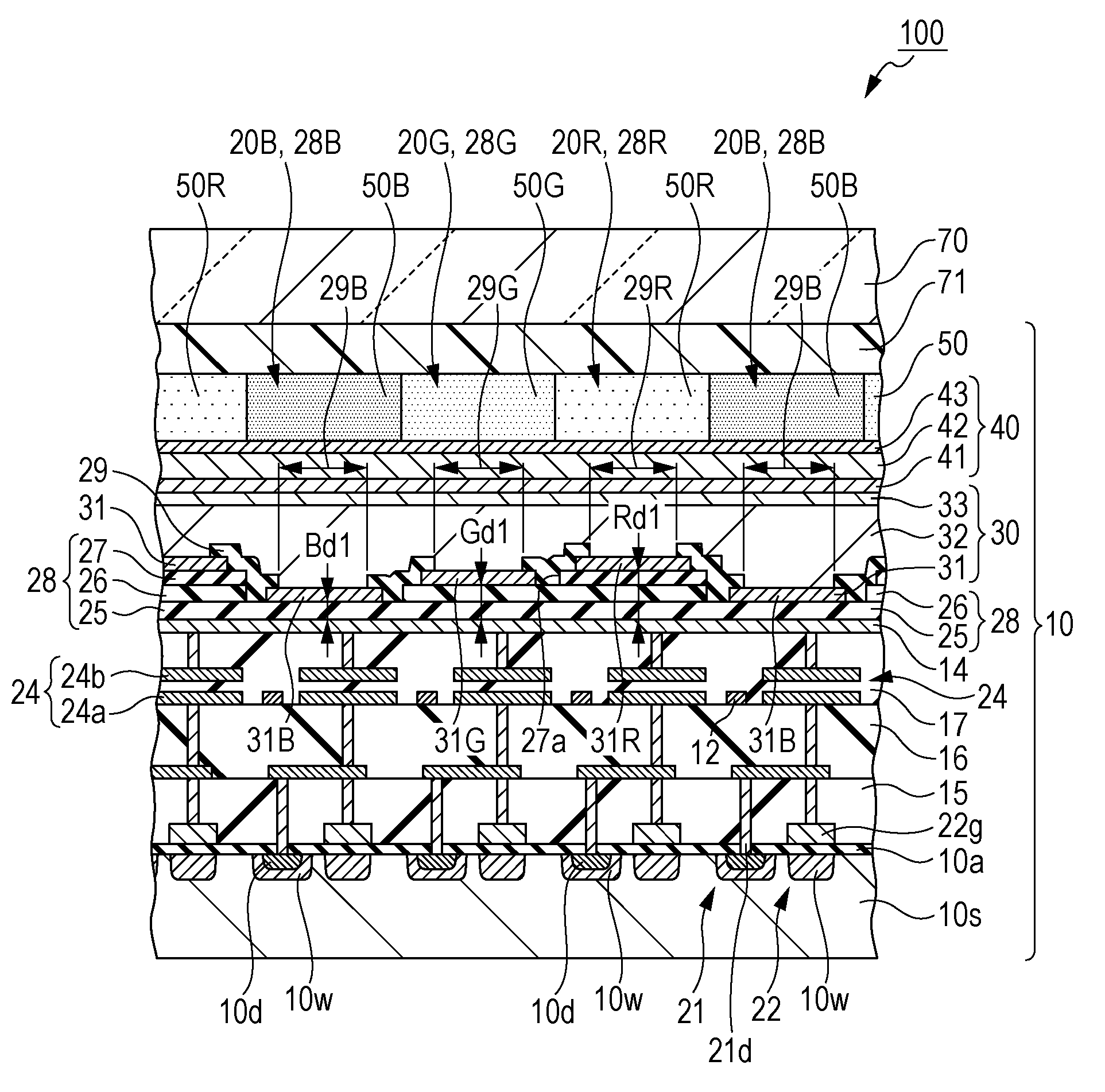
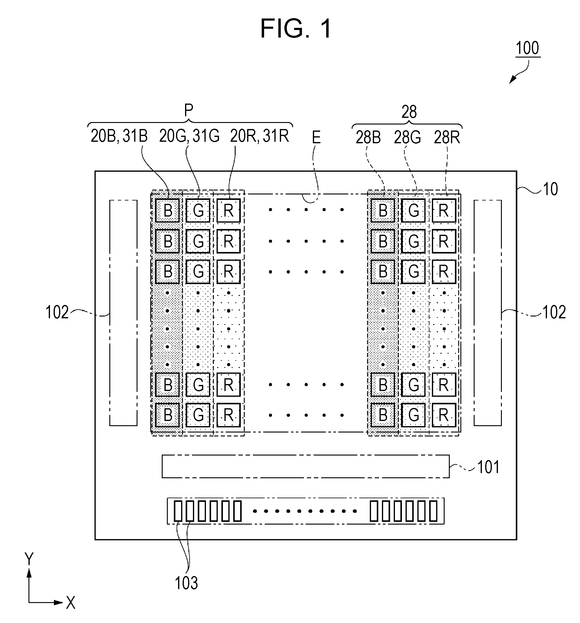
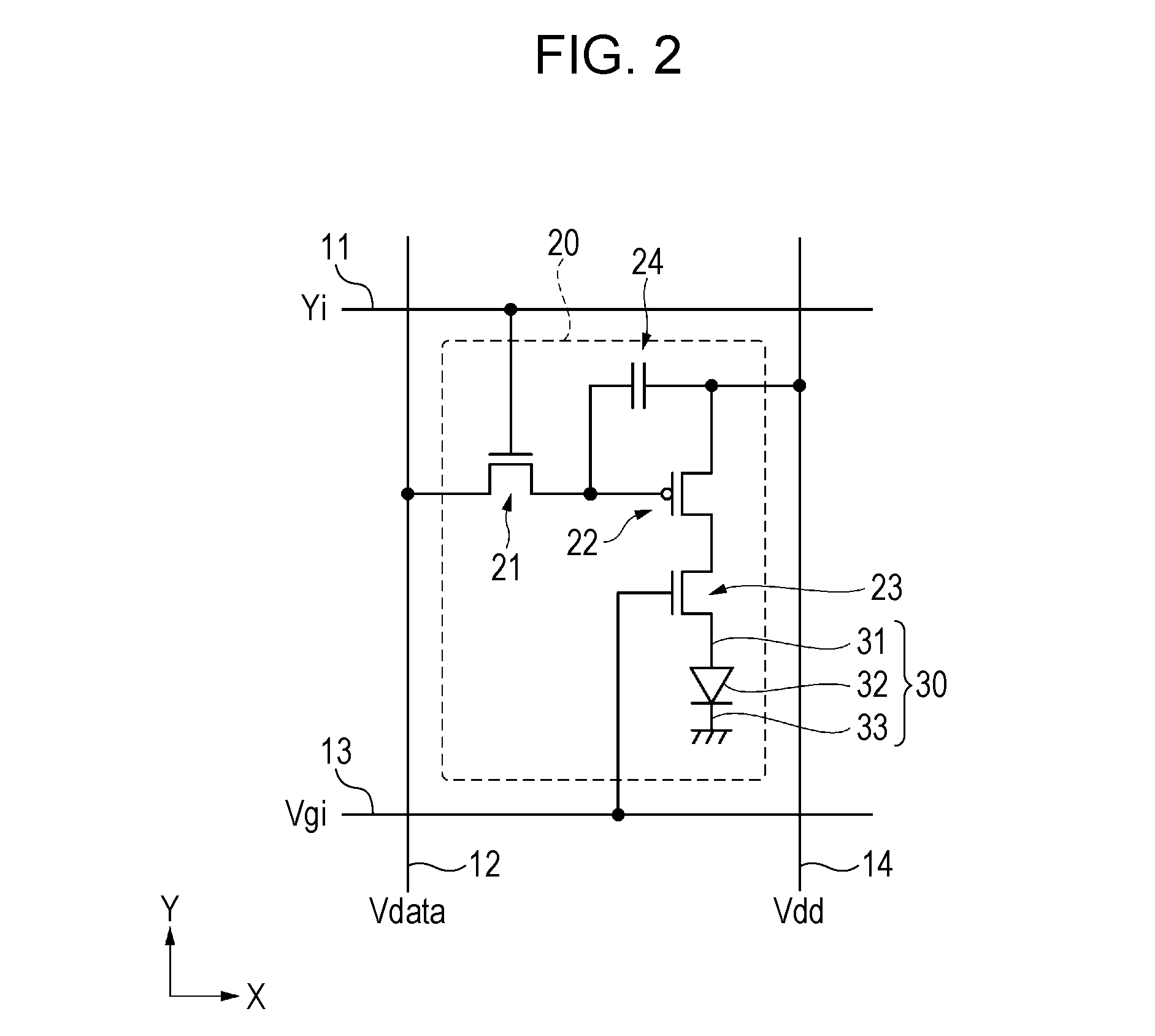
[0062]First, the outline of the organic EL apparatus 100 according to the embodiment will be described with reference to FIGS. 1 to 3. FIG. 1 is a schematic plane view illustrating the configuration of the organic EL apparatus, FIG. 2 is an equivalent circuit diagram illustrating the electrical configuration of the organic EL apparatus, and FIG. 3 is a schematic plane view illustrating a characteristic portion of the light emitting pixels.

[0063]Meanwhile, FIG. 3 illustrates components which are necessary to describe the characteristic portion of the light emitting pixels and does not illustrate the other components. In addition, in FIG. 3, two-dot dashed lines show the outlines of the light emitting pixels 20.

[0064]As shown in FIG. 1...

second embodiment

Outline of Organic EL Apparatus

[0202]FIG. 12 is a schematic cross-sectional diagram illustrating the configuration of an organic EL apparatus according to a second embodiment with regard to FIG. 4, that is, a schematic cross-sectional diagram illustrating an area, in which the openings are provided, in the second insulation layer which defines a light emission area. FIG. 13 is another schematic cross-sectional diagram illustrating the configuration of the organic EL apparatus according to the second embodiment with regard to FIG. 5, that is, a schematic cross-sectional diagram illustrating an area in which the pixel electrode is electrically connected to the third transistor.

[0203]Hereinafter, the outline of the organic EL apparatus 200 according to the embodiment will be described with reference to FIGS. 12 and 13 centering on the difference from the first embodiment. Meanwhile, the same reference numerals are attached to the same components as in the first embodiment, and the desc...

third embodiment

Electronic Equipment

[0229]FIG. 17 is a schematic diagram illustrating a head mounted display as an example of electronic equipment.

[0230]As shown in FIG. 17, a head mounted display 1000 includes two display units 1001 which are provided to correspond to the right and left eyes. When an observer M mounts the head mounted display 1000 on the head like glasses, the observer M can see letters, images, and the like which are displayed on the display units 1001. For example, if images are displayed in consideration of the parallax between the right and left display units 1001, it is possible to see and enjoy stereoscopic images.

[0231]In the display units 1001, the organic EL apparatus 100 according to the first embodiment or the organic EL apparatus 200 according to the second embodiment is mounted. Since the organic EL apparatus 100 and the organic EL apparatus 200 include the optical resonance structure, the color purity of light which is emitted from the light emitting pixels 20B, 20G,...


PUM


Abstract

A light emitting device includes a transistor, a light reflection layer, a first insulation layer that includes a first layer thickness part, a second layer thickness part, and a third layer thickness part, a pixel electrode that is provided on the first insulation layer, a second insulation layer that covers a peripheral section of the pixel electrode, a light emission functional layer, a facing electrode, and a conductive layer that is provided on the first layer thickness part. The pixel electrode includes a first pixel electrode which is provided in the first layer thickness part, a second pixel electrode which is provided in the second layer thickness part, and a third pixel electrode which is provided in the third layer thickness part. The first pixel electrode, the second pixel electrode, and the third pixel electrode are connected to the transistor through the conductive layer.

Description

BACKGROUND[0001]1. Technical Field[0002]The present invention relates to a light emitting device, a method of manufacturing the light emitting device, and electronic equipment in which the light emitting device is mounted.[0003]2. Related Art[0004]As an example of a light emitting device, for example, an electro-optic device, in which organic Electroluminescent (hereinafter, referred to as an organic EL) elements are arranged in a matrix shape (JP-A-2009-134067), has been proposed. The electro-optic device disclosed in JP-A-2009-134067 is an active matrix type light emitting device which includes a thin film transistor and in which pixels for emitting light are arranged in a matrix shape. In the pixels, a light reflection layer, a translucent insulation film, a first electrode (pixel electrode), a barrier layer, a light emission functional layer, and a second electrode (facing electrode) are sequentially laminated.[0005]A current is supplied to the light emission functional layer fr...

Claims


Application Information

Patent Timeline
Patent Type & Authority Patents(United States)
IPC IPC(8): H01L29/08H01L29/20H01L29/24H01L29/00H01L27/32H01L27/14H01L51/52
CPCH01L27/3248H01L27/3258H01L51/5265H01L27/3206H01L51/5271H01L2227/323H01L2251/5315H01L2251/5392H10K59/30H10K59/35H10K59/123H10K59/124H10K50/852H10K50/856H10K59/1201H10K2102/3026H10K2102/341H10K59/1213H10K59/38H10K59/126H10K50/00H10K50/805H10K50/818H10K50/824H10K59/351
Inventor KOSHIHARA, TAKESHINOZAWA, RYOICHI
Owner SEIKO EPSON CORP
Why Eureka
Try Eureka