Fast turn on system for a synthesized source signal

a compensation system and signal source technology, applied in multiplex communication, gain control, gated amplifiers, etc., can solve the problems of narrow loop bandwidth of high-quality vco's, difficult isolation of vco and mute amplifiers, and disturbance of the phase of synthesized signal source, so as to reduce the phase disturbance of the rf output signal.

Active Publication Date: 2015-10-27
HITTITE MICROWAVE LLC
View PDF14 Cites 1 Cited by
  • Summary
  • Abstract
  • Description
  • Claims
  • Application Information

AI Technical Summary

Benefits of technology

[0009]In one embodiment, the mute amplifier and the dummy amplifier may each be configured to draw the same amount of power supply current from the power supply when enabled. The mute amplifier and the dummy amplifier may each be coupled to synthesized signal source. The combined impedance of the mute amplifier and the dummy amplifier presented to the synthesized signal source may be configured to be approximately constant before, during, and after enabling the mute amplifier. The mute amplifier may be differentially coupled to RF output signal load and a complementary output signal load to reduce electromagnetic coupling between the RF output signal and the synthesized signal source. The mute amplifier input may be coupled to synthesized signal source. The system may include a buffer amplifier coupled between the mute amplifier and the synthesized signal source configured such that the impedance presented to the synthesized signal source is approximately constant before, during, and after enabling the mute amplifier and the synthesized signal source is isolated from the mute amplifier to reduce the effects of change in input impedance of the mute amplifier at the synthesized signal source when the mute amplifier is enabled. The synthesized signal source, the mute amplifier, the dummy amplifier, and the mute controller may be located on an integrated circuit chip. The synthesized signal source may include a phase lock loop. The synthesized signal source may be coupled to and responsive to a reference signal generator.
[0011]In one embodiment, the mute amplifier and the dummy amplifier may each be configured to draw the same amount of current from the power supply when enabled. The mute amplifier and the dummy amplifier may each be coupled to synthesized signal source. The mute amplifier may be differentially coupled to the RF output signal load and a complementary output signal load to reduce electromagnetic coupling between the RF output signal and the synthesized signal source. The mute amplifier input may be coupled to synthesized signal source. The system may include a buffer amplifier coupled between the mute amplifier and the synthesized signal source configured such that the impedance presented to the synthesized signal source is approximately constant before, during, and after enabling the mute amplifier and the synthesized signal source is isolated from the mute amplifier to reduce the effects of change in input impedance of the mute amplifier impedance at the synthesized signal source when the mute amplifier is enabled. The synthesized signal source, the mute amplifier, the dummy amplifier, and the mute controller may be located on an integrated circuit chip. The synthesized signal source may include a phase lock loop. The synthesized signal source may be coupled to and responsive to a reference signal generator.
[0012]In another aspect, a fast turn on compensation system for a synthesized signal source is featured. A synthesized signal source is coupled to a power supply and configured to generate a phase stable radio frequency (RF) output signal. A mute amplifier is coupled to the synthesized signal source and the power supply. A dummy amplifier is coupled to the mute amplifier and the power supply and located in close proximity to the mute amplifier. A mute controller is coupled to the mute amplifier and the dummy amplifier, the mute controller is responsive to an enable signal and configured to enable the dummy amplifier and disable the mute amplifier when no RF output signal is being generated and disable the dummy amplifier and enable the mute amplifier when the RF output signal is being generated such that total power supply current delivered to the synthesized signal source and the enabled dummy amplifier or mute amplifier and the combined impedance of the mute amplifier and the dummy amplifier presented to the synthesized signal source is approximately constant before, during, and after enabling the mute amplifier to reduce phase disturbance of the RF output signal. The mute amplifier is differentially coupled to the RF output signal load and a complementary output signal load to reduce electromagnetic coupling between the RF output signal and the synthesized signal source.
[0013]In one embodiment, the mute amplifier and the dummy amplifier may each be configured to draw the same amount of current from the power supply when enabled. The system may include a buffer amplifier coupled between the mute amplifier and the synthesized signal source configured such that the impedance presented to the synthesized signal source is approximately constant before, during, and after enabling the mute amplifier and the synthesized signal source is isolated from the mute amplifier to reduce the effects of change in input impedance of the mute amplifier at the synthesized signal source when the mute amplifier is enabled. The synthesized signal source, the mute amplifier, the dummy amplifier, and the mute controller may be located on an integrated circuit chip. The synthesized signal source may include a phase lock loop. The synthesized signal source may be coupled to and responsive to a reference signal generator.

Problems solved by technology

When the mute amplifier is enabled, it draws current from the power supply which disturbs the locked voltage controlled oscillator (VCO) of the synthesized signal source.
This causes a disturbance in the synthesized signal source phase, which may jump at the turn on instant and decay slowly back to some final phase.
Isolation of the VCO and mute amplifier is difficult in small integrated circuits or with large discrete VCOs.
Additionally, high quality VCO's may have narrow loop bandwidths, which have long settling times if disturbed.
Such a design may result in electromagnetic coupling of the RF field created by the VCO and the RF field created by the mute amplifier.
Such RF field coupling may create a phase disturbance or “wobble” and often results in a transient phase that moves slowly to a new steady state phase, which is typically at a different phase from the phase before the enable, known as phase disturbance.
This changes the impedance seen by the VCO which also creates a phase disturbance.
However, such circuits suffer from the problem that when the loop bandwidth is changed from fast to slow, the final phase offset is altered and the result is a phase transient that causes a long undesired settling time.

Method used


Image

  • Fast turn on system for a synthesized source signal
  • Fast turn on system for a synthesized source signal
  • Fast turn on system for a synthesized source signal

Examples


Embodiment Construction

[0021]Aside from the preferred embodiment or embodiments disclosed below, this invention is capable of other embodiments and of being practiced or being carried out in various ways. Thus, it is to be understood that the invention is not limited in its application to the details of construction and the arrangements of components set forth in the following description or illustrated in the drawings. If only one embodiment is described herein, the claims hereof are not to be limited to that embodiment. Moreover, the claims hereof are not to be read restrictively unless there is clear and convincing evidence manifesting a certain exclusion, restriction, or disclaimer.

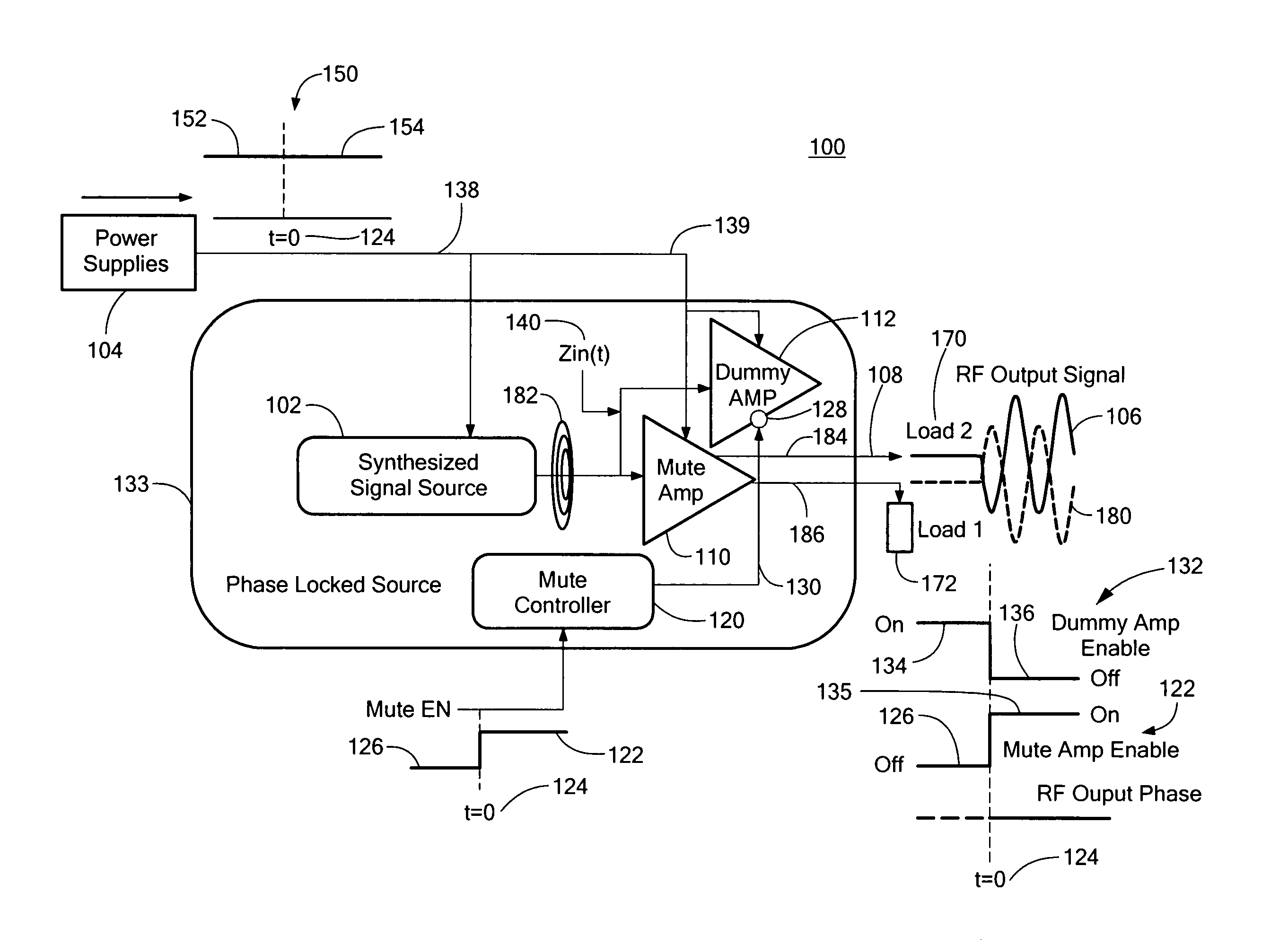
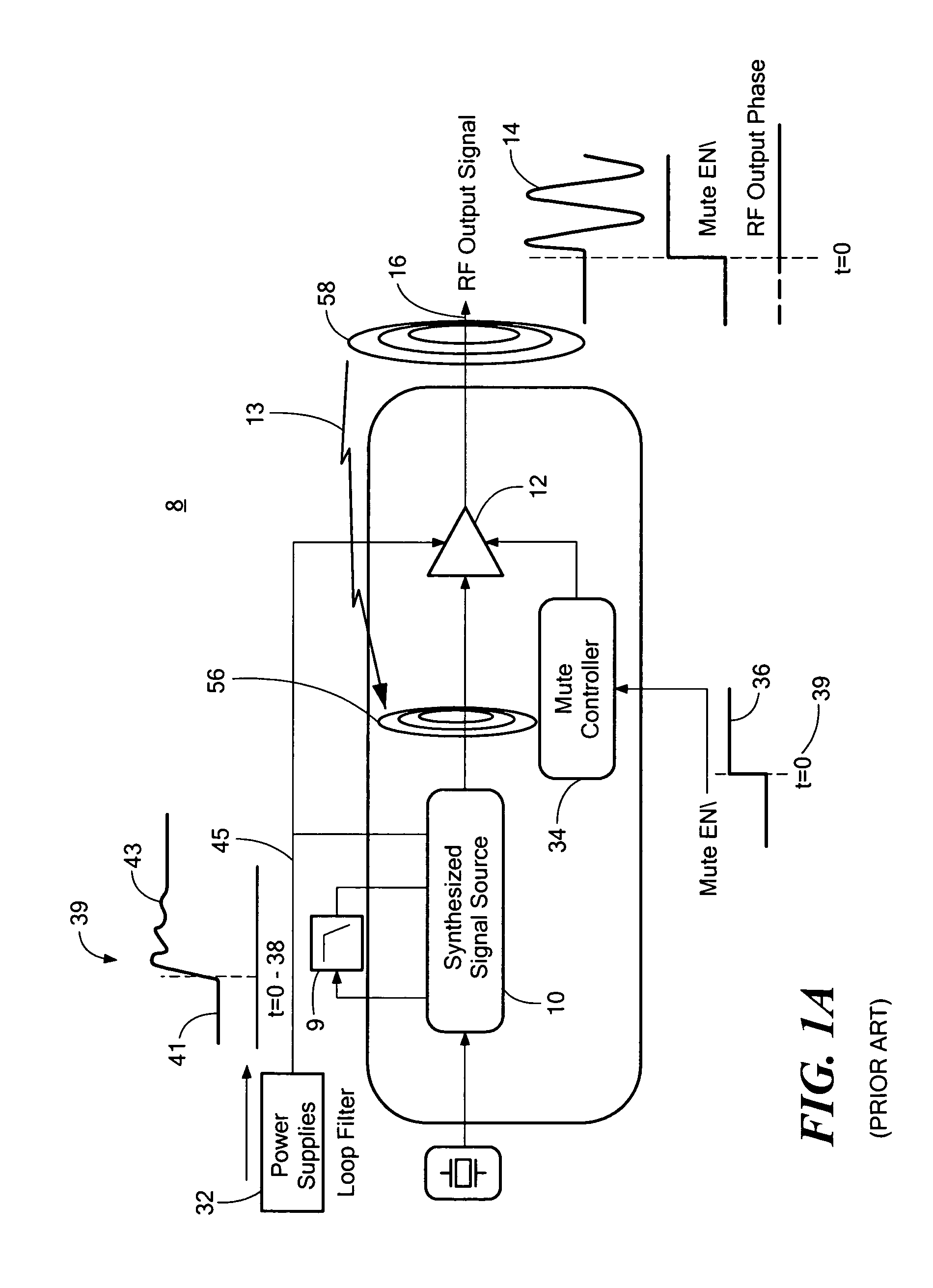
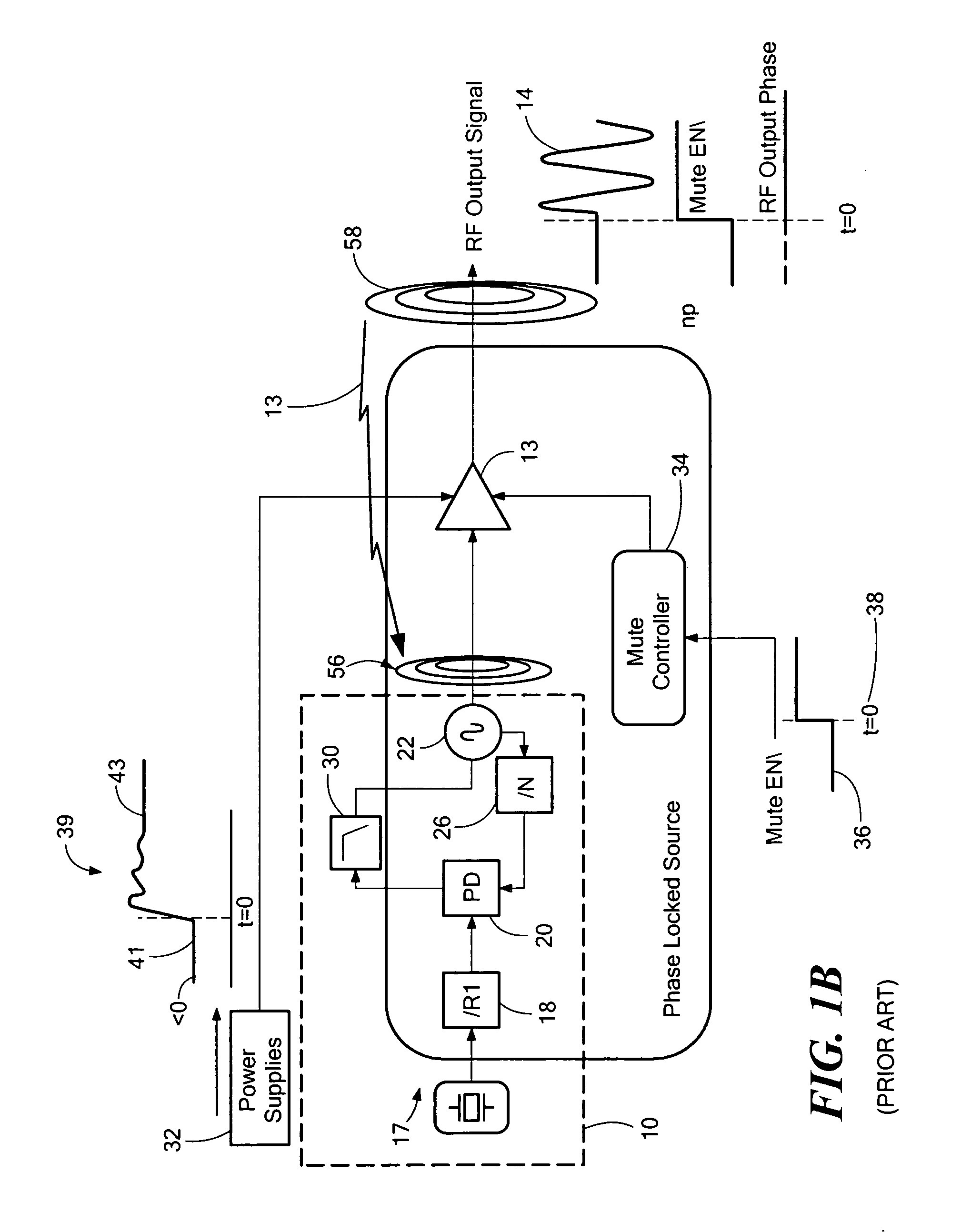
[0022]Conventional synthesized source system 8, FIG. 1A, includes synthesized signal source 10 coupled to mute amplifier 12 configured to generate a phase stable RF output signal 14 on line 16. As disclosed herein, a synthesized signal source, such as synthesized source signal 10, may be as phase lock loop (PLL), phase lock...


PUM


Abstract

A fast turn on compensation system for a synthesized signal source includes a synthesized signal source coupled to a power supply and configured to generate a phase stable radio frequency (RF) output signal. A mute amplifier is coupled to the synthesized signal source and the power supply. A dummy amplifier is coupled to the mute amplifier and the power supply. A mute controller is coupled to the mute amplifier and the dummy amplifier, the mute controller is responsive to an enable signal and configured to enable the dummy amplifier and disable the mute amplifier when no RF output signal is being generated and disable the dummy amplifier and enable the mute amplifier when the RF output signal is being generated such that total power supply current delivered to the synthesized signal source and the dummy amplifier or mute amplifier is approximately constant before, during, and after enabling the mute amplifier to reduce phase disturbance of the RF output signals.

Description

FIELD OF THE INVENTION[0001]This invention relates to fast turn on compensation system for a synthesized signal sourceBACKGROUND OF THE INVENTION[0002]A synthesized signal source, e.g., a phase lock loop (PLL), a phase locked voltage controlled oscillator (VCO) or similar type device, is often coupled to an output buffer or mute amplifier. The output buffer or mute amplifier turns the RF (Radio Frequency) output signal from the synthesized signal source on and off, isolates the output from the input, and provides RF output power as required by systems attached to it.[0003]It is often desirable to be able to quickly turn on or turn off the synthesized signal source output. This is often necessary for Time Division Multiple Access (TDMA) systems requiring blanking between communication intervals (packets), such as in the GSM system. It is often desirable to have a near zero phase disturbance at turn on, e.g., less than about 5° of phase variation on the output signal phase, e.g., with...

Claims


Application Information

Patent Timeline
Patent Type & Authority Patents(United States)
IPC IPC(8): H04J3/06H03L7/00H03F3/00
CPCH03L7/00H03F3/00H03F1/30H03F3/72H03F2200/453H03G3/348H03F3/195H03F3/45475H03F2200/451H03F2200/459
Inventor CLOUTIER, MARK M.BACHMANEK, GREGPAMIR, TOLGA
Owner HITTITE MICROWAVE LLC
Why Eureka
Try Eureka