Production of a semiconductor device having at least one column-shaped or wall-shaped semiconductor element

a semiconductor element and column-shaped technology, applied in the direction of semiconductor devices, basic electric elements, electrical equipment, etc., can solve problems such as control of procedural parameters, and achieve the effects of avoiding disadvantages of conventional methods, improving accuracy and/or reproducibility, and simplifying the procedur

Active Publication Date: 2015-11-10
FORSCHUNGSVERBUND BERLIN EV
View PDF11 Cites 9 Cited by
  • Summary
  • Abstract
  • Description
  • Claims
  • Application Information

AI Technical Summary

Benefits of technology

[0008]The objective of the invention is to provide an improved method of producing a semiconductor device, which comprises a structured semiconductor, with which disadvantages of conventional methods can be avoided. The objective of the invention is in particular to provide a method of producing a semiconductor device with nanostructured semiconductor elements which is characterised by a simplified procedure. The method should also allow increased accuracy and/or reproducibility of the

Problems solved by technology

In particular the adjustment of the emission of a specific spectral range, e.g. the adjustment of a white light emission, constitutes a great challenge for the control of procedural parameters in the production of the nanostructured semiconductor

Method used


Image

  • Production of a semiconductor device having at least one column-shaped or wall-shaped semiconductor element
  • Production of a semiconductor device having at least one column-shaped or wall-shaped semiconductor element
  • Production of a semiconductor device having at least one column-shaped or wall-shaped semiconductor element

Examples


Embodiment Construction

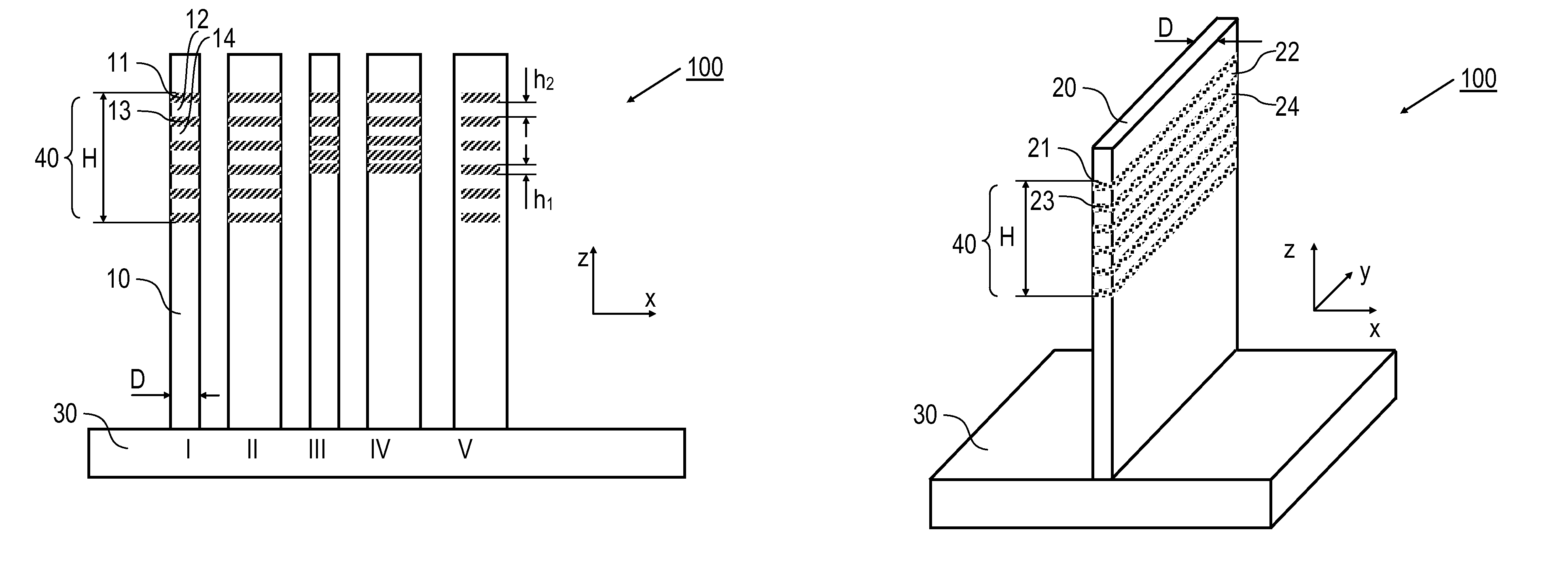
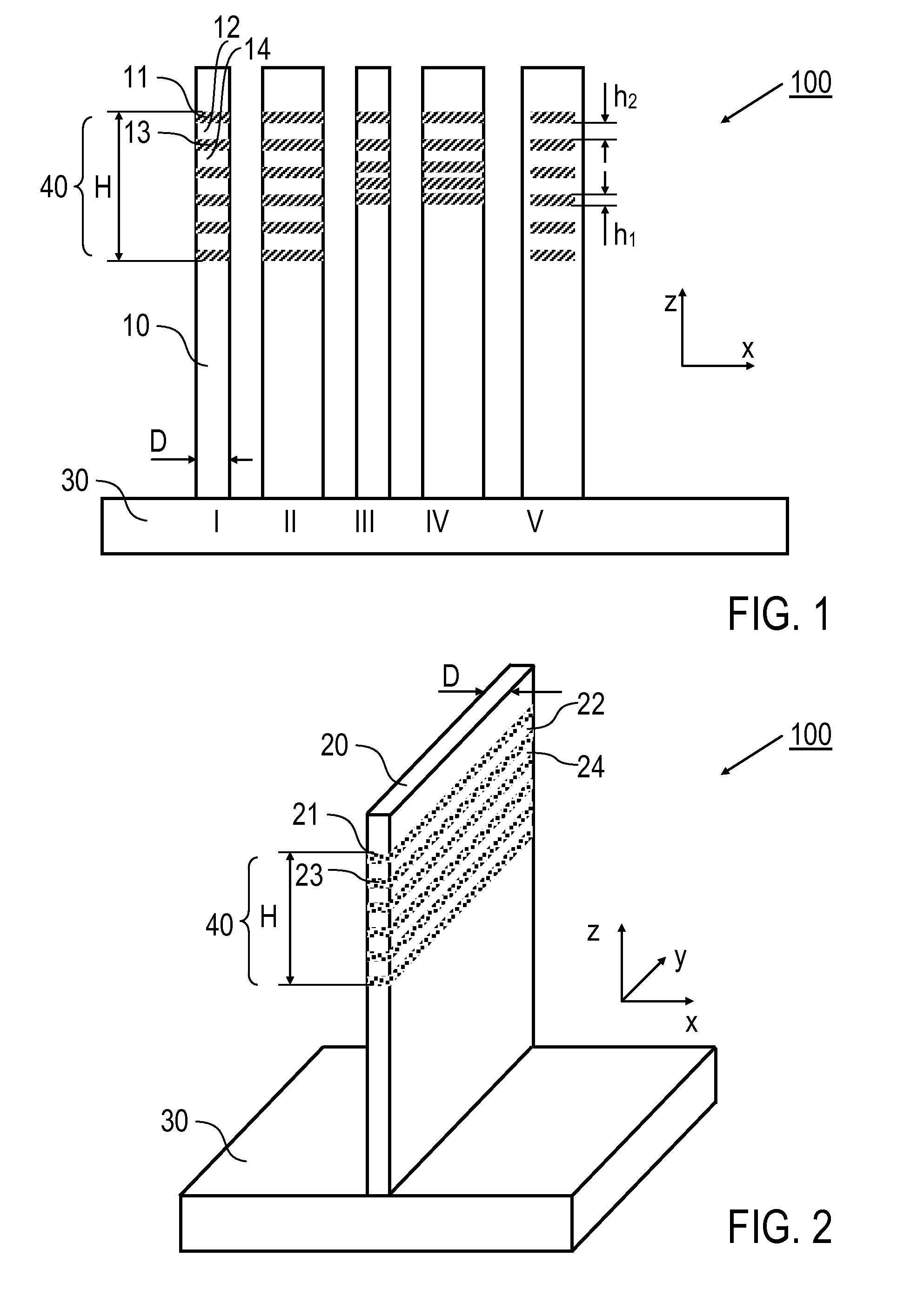
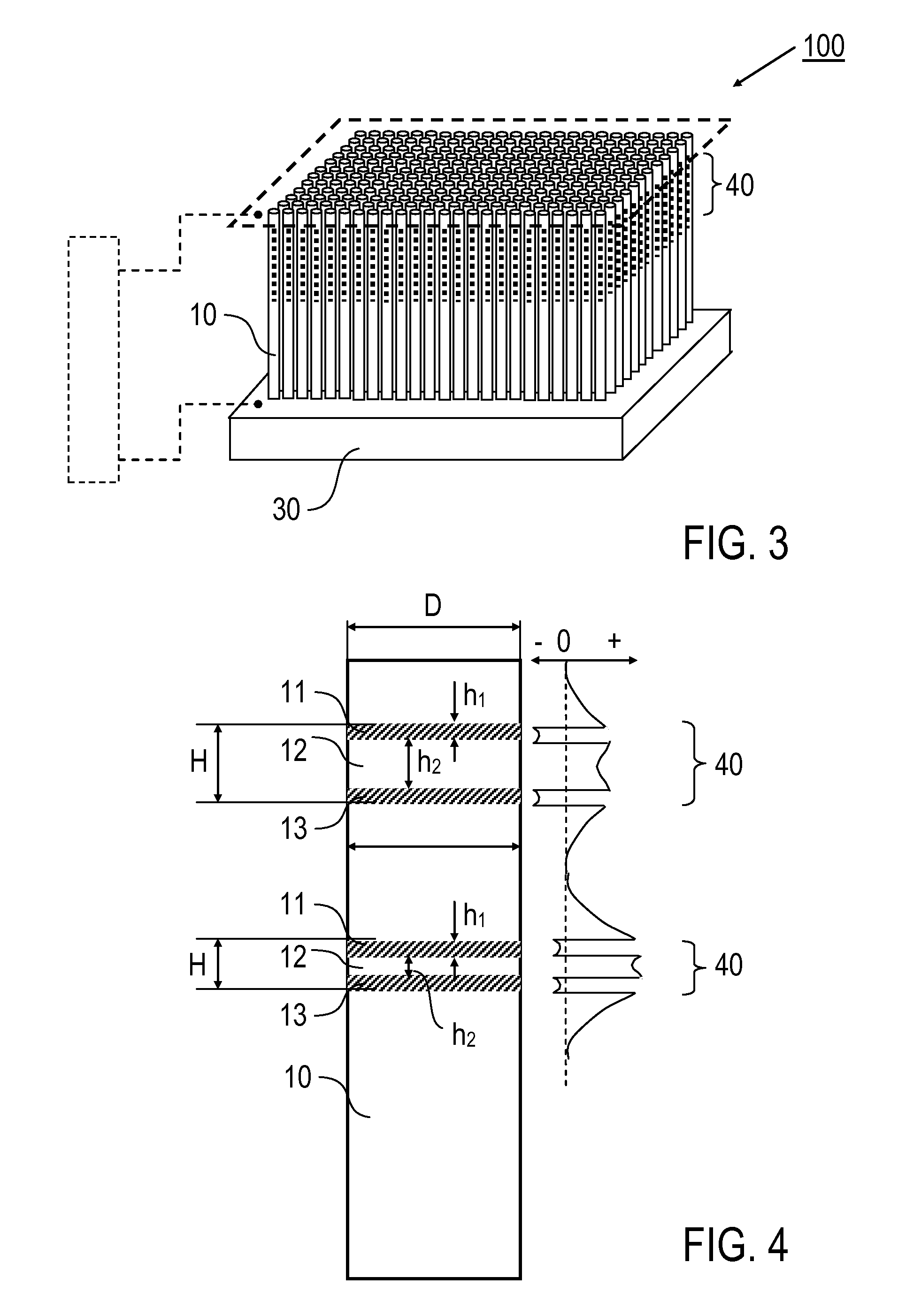
[0010]According to general aspects of the invention, the above objectives are each solved by a method for producing a semiconductor device or by a semiconductor device, whereby the semiconductor device comprises a substrate and at least one semiconductor element, which has an elongated shape and which extends in a main direction which deviates from the extension of the surface of the substrate. The semiconductor element is characterised by a lateral thickness across the main direction which is less than the height (length) of the semiconductor element in the main direction. The elongated shape of the semiconductor element is formed such that the semiconductor element in at least one section plane has an aspect ratio (quotient of lateral thickness and length) of less than 1, preferably less than 0.1, and by special preference less than 0.05. The basic shapes of the semiconductor element are, for example, the shape of a column (or needle, wire or rod) or the shape of a wall (or disc)....


PUM


Abstract

Described is a method for producing a semiconductor device (100), in which at least one column-shaped or wall-shaped semiconductor device (10, 20) extending in a main direction (z) is formed on a substrate (30), wherein at least two sections (11, 13, 21, 23) of a first crystal type and one section (12, 22) of a second crystal type therebetween are formed in an active region (40), each section with a respective predetermined height (h1, h2), wherein the first and second crystal types have different lattice constants and each of the sections of the first crystal type has a lattice strain which depends on the lattice constants in the section of the second crystal type. According to the invention, at least a height (h2) of the section (12, 22) of the second crystal type and a lateral thickness (D) of the active region (40) is formed perpendicular to the main direction, in such a manner that the lattice strain in one of the sections (11) of the first crystal type also depends on the lattice constants in the other section (13) of the first crystal type. A semiconductor device (100) is also described, having at least one column-shaped or wall-shaped semiconductor element (10, 20) on a substrate (30), which can be produced in particular by means of the stated method.

Description

BACKGROUND OF THE INVENTION[0001]The invention refers to a method for the production of a semiconductor device such as a light-emitting component, having at least one column-shaped or wall-shaped semiconductor element, and in particular refers to a method for the production of a semiconductor device where at least one semiconductor element has a lateral thickness in at least one cross-section direction of less than 1 μm, in particular less than 500 nm. The invention furthermore refers to a semiconductor device having at least one column-shaped or wall-shaped semiconductor element, in particular a semiconductor device with at least one nanowire and / or at least one nanowall which is arranged on a substrate. Applications for the invention exist in the production of optical, in particular light emitting, electrical, electromechanical and / or electro-thermal components.[0002]The production of semiconductor elements (nanostructured semiconductor elements) on a substrate which have characte...

Claims


Application Information

Patent Timeline
IPC IPC(8): H01L21/00H01L29/20H01L31/0352H01L33/06H01L29/16H01L29/04H01L33/18H01L29/12H01L31/109H01L27/15H01L29/06
CPCH01L29/122H01L29/04H01L29/16H01L29/20H01L29/2003H01L31/035209H01L33/06H01L33/18H01L2924/0002H01L2924/00
Inventor BRANDT, OLIVERGEELHAAR, LUTZKAGANER, VLADIMIRWOELZ, MARTIN
Owner FORSCHUNGSVERBUND BERLIN EV
Why Eureka
Try Eureka