Ultrasonic sensor microarray and method of manufacturing same

a technology of ultrasonic sensor and microarray, which is applied in the direction of microstructural devices, mechanical vibration separation, coatings, etc., can solve the problems that the production of arrays of cmut sensors or transducers on a commercial scale has not received widespread penetration in the marketplace, and achieves a wide range of output beam shape and/or configuration

Active Publication Date: 2015-11-17
UNIVERSITY OF WINDSOR
View PDF24 Cites 1 Cited by
  • Summary
  • Abstract
  • Description
  • Claims
  • Application Information

AI Technical Summary

Benefits of technology

[0012]It is envisioned that the invention may provide a simplified and reliable method of manufacturing CMUT microarray modules in an ultrasonic sensor manufacturing process, in which multiple CMUT microarrays modules may be more easily provided either in a hyperboloid parabolic geometry using a molding, stamping or three dimensional (3D) printing process; or which simulates such a configuration.
[0014]Preferably, the sensor assembly includes at least one CMUT microarray module which incorporates a number of individual transducer / sensors, and which are activatable individually, selectively or collectively to emit and receive reflected signals. Most preferably in the assembly of the wafer construct, BCB is applied to opposing surfaces of adjacent silicon or other wafers which are to be joined, and semi-cured to achieve BCB-wafer to BCB-wafer surface adherence. In a most preferred mode of assembly, the BCB layers are reduced and / or thinned using a suitable thinner such as Mesitylene (1,3,5-trimethylbenzene). The thinned BCB resin may be spin deposited to create a desired thickness build up having regard to the final Z-height of the wafer construct to be achieved. The applicant has appreciated that the present method allows for final curing of the BCB layers at lower temperatures and / or over long time intervals operate to reduce heat stress to the assembled wafer construct.
[0016]In one construction, the microarray modules are mounted to a backing in a substantially flat geometry, and which preferably has a curvature of less than ±10°, and more preferably less than ±1°. Whilst sensor assemblies may include as few as a single microarray module, more preferably multiple CMUT microarray modules are provided, and which are arranged in a square matrix module arrangement of 9×9 or greater. Optionally, individual CMUT microarray modules may be formed as a generally flexible sheet which allows for free-form shaping, to permit a greater range of output beam shape and / or configurations.

Problems solved by technology

As a result, the production of arrays of CMUT sensors or transducers on a commercial scale has yet to receive widespread penetration in the marketplace.

Method used


Image

  • Ultrasonic sensor microarray and method of manufacturing same
  • Ultrasonic sensor microarray and method of manufacturing same
  • Ultrasonic sensor microarray and method of manufacturing same

Examples


Embodiment Construction

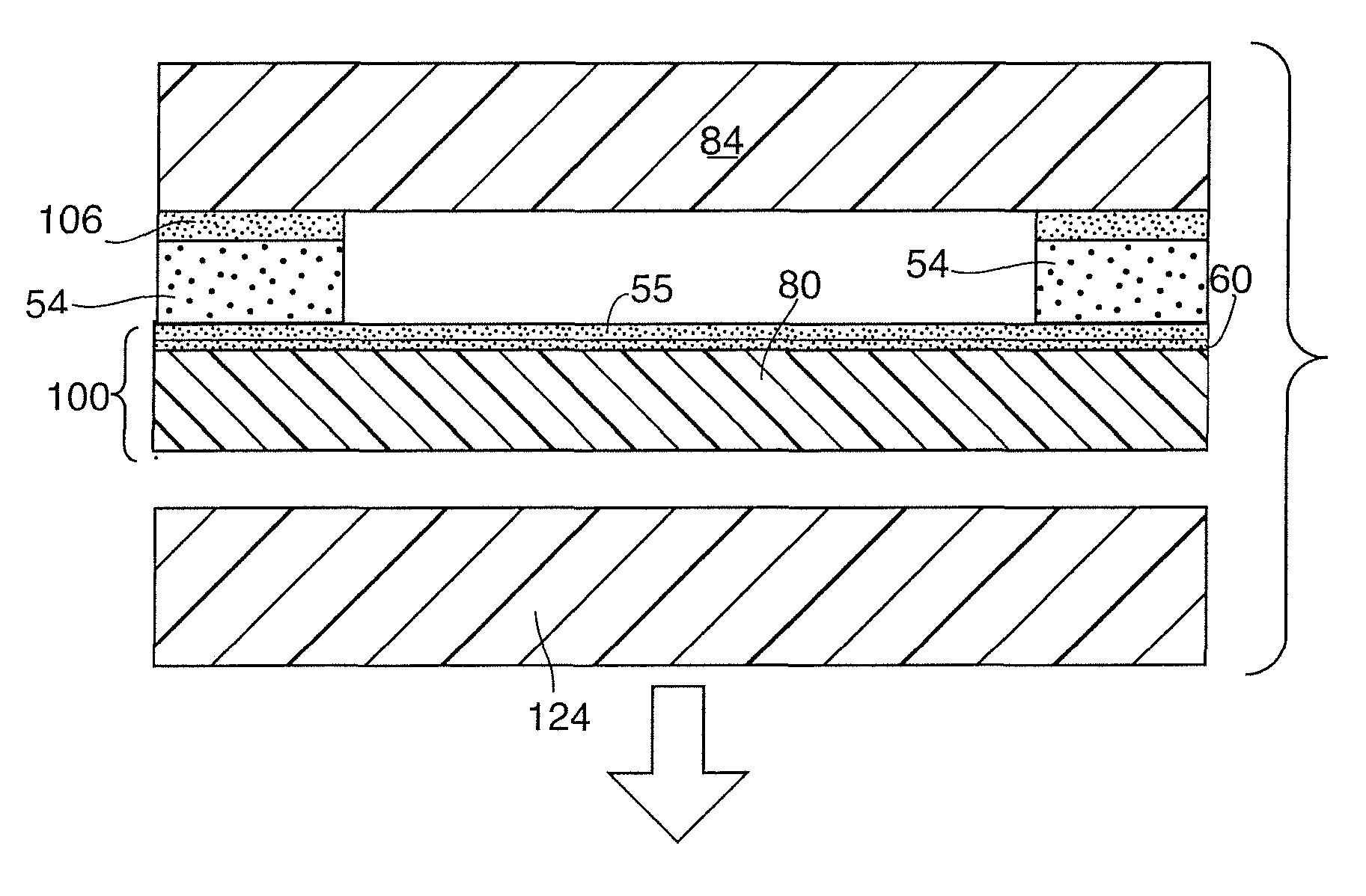
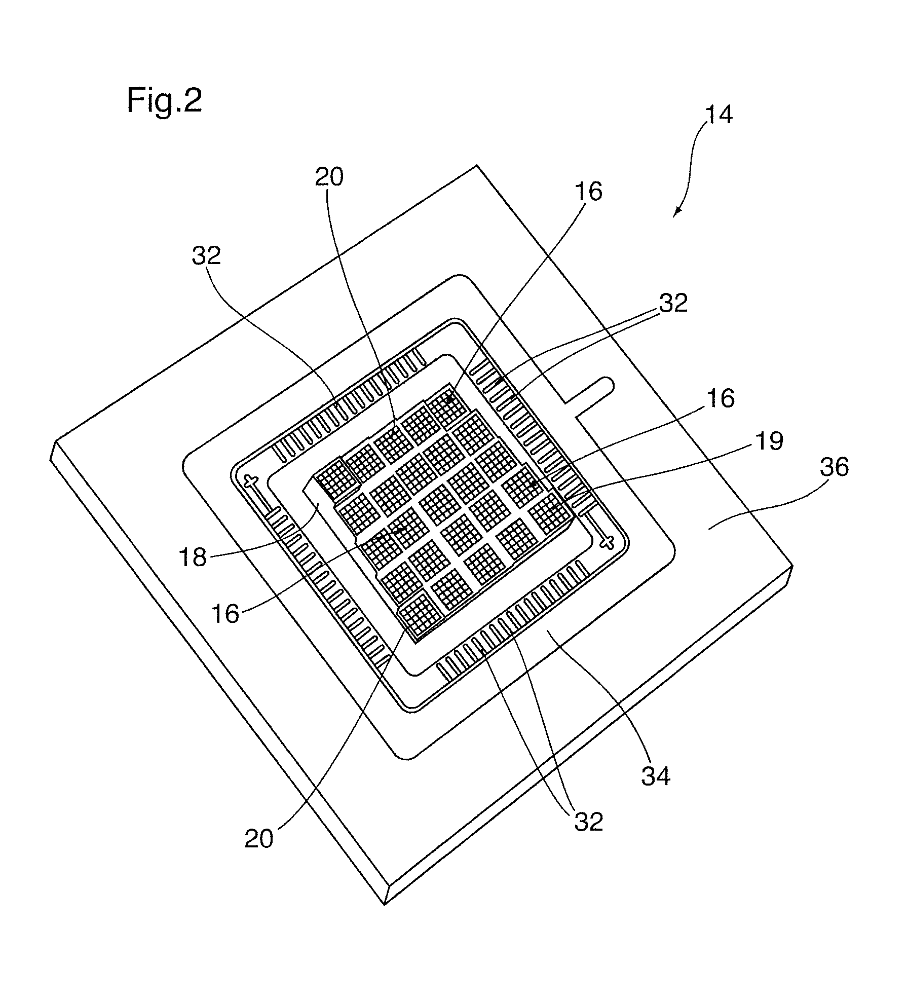
[0057]In accordance with a most preferred process, benzocyclobutene is provided as both a structural component and adhesive used in the bonding of one or more silicon and silicon-on-insulator (SOI) (shown as 20 in FIG. 5) wafers in the manufacture of MEMS devices, and most preferably CMUT transducers. Most preferably the CMUT transducer 20 is provided as part of a series of individual CMUT transducers which are arranged in an array, and preferably at least a 6×6 array, preferably at least a 10×10 array, and more preferably approximately 40×40 square array configuration.

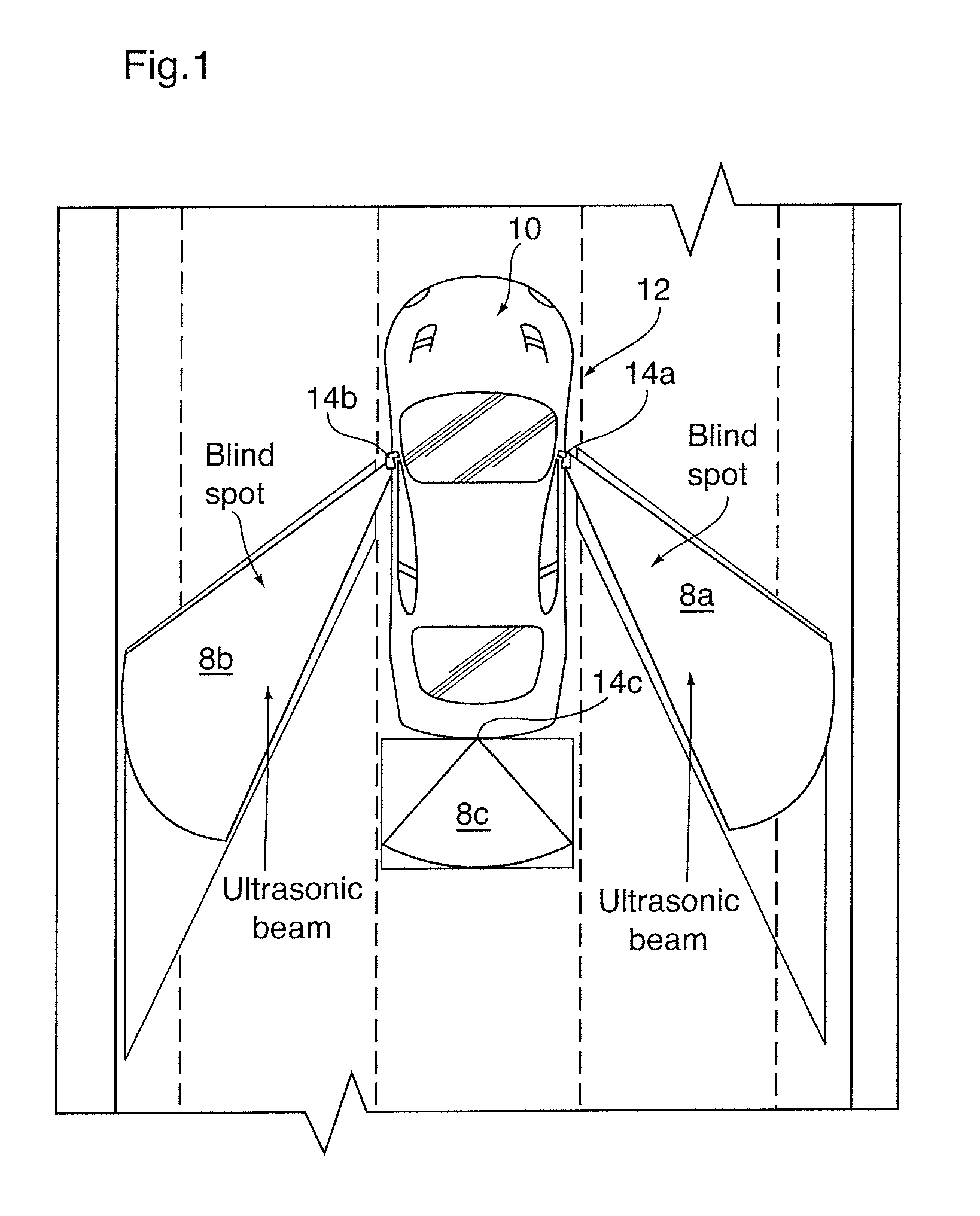
[0058]As will be described, the transducers 20 may operate with suitable frequency ranges may be as low as 40 kHz. In vehicle applications, more preferably the transducer / sensor of each microarray is operable at frequencies of at least 100 kHz, and most preferably at about 150 kHz to minimize the effects of air damping. In a preferred construction, the sensor assembly is provided for operation as vehicle blind-spot se...


PUM

PropertyMeasurementUnit
thicknessaaaaaaaaaa
thicknessaaaaaaaaaa
depthaaaaaaaaaa

Abstract

A sensor assembly including one or more capacitive micromachined ultrasonic transducer (CMUT) microarray modules which are provided with a number of individual transducers. The transducers include silicon device and backing layers joined by a fused benzocyclobutene (BCB) layer which defines the transducer air gap, and which are arranged to simulate or orient individual transducers in a hyperbolic paraboloid geometry. The transducers / sensor are arranged in a matrix and are activatable to emit and receive reflected beam signals at a frequency of between about 100 to 170 kHz.

Description

RELATED APPLICATIONS[0001]This application claims priority and the benefit of 35 USC §119(e) to U.S. Patent Application Ser. No. 61 / 856,224, filed 19 Jul. 2013.SCOPE OF THE INVENTION[0002]The present invention relates to a microelectromechanical system (MEMS) and its method of manufacture, and more particularly three-dimensional MEMS devices such as sensor microarrays which may function as part of a capacitive micromachined ultrasonic transducer (CMUT). In a preferred application, the present invention relates to a method of manufacturing an ultrasonic sensor microarray which simulates a hyperbolic paraboloid shaped sensor configuration or chip, and which includes bonding partially cured benzocyclobutene (BCB) layers as a structural component. Suitable uses for the CMUT include non-vehicular and / or vehicle or automotive sensor applications, as for example in the monitoring of vehicle blind-spots, obstructions and / or in autonomous vehicle drive and / or parking applications.BACKGROUND ...

Claims


Application Information

Patent Timeline
Patent Type & Authority Patents(United States)
IPC IPC(8): H01L21/00B81C1/00
CPCB81C1/00269H01L2924/1461B06B1/0292
Inventor CHOWDHURY, SAZZADURBAKHTAZAD, AREF
Owner UNIVERSITY OF WINDSOR
Why Eureka
Try Eureka