

Three-dimensional stacked structured ASIC devices and methods of fabrication thereof
a technology of structured asic devices and integrated circuits, applied in semiconductor devices, semiconductor/solid-state device details, electrical apparatus, etc., can solve the problems of increasing the fabrication duration and cost of total devices, and the 3d integration could increase the total device fabrication duration and cost, and achieves low parasitic effects, facilitates silicon photonics integration, and high density
- Summary
- Abstract
- Description
- Claims
- Application Information
AI Technical Summary
Benefits of technology
Problems solved by technology
Method used
Image

Examples
Embodiment Construction
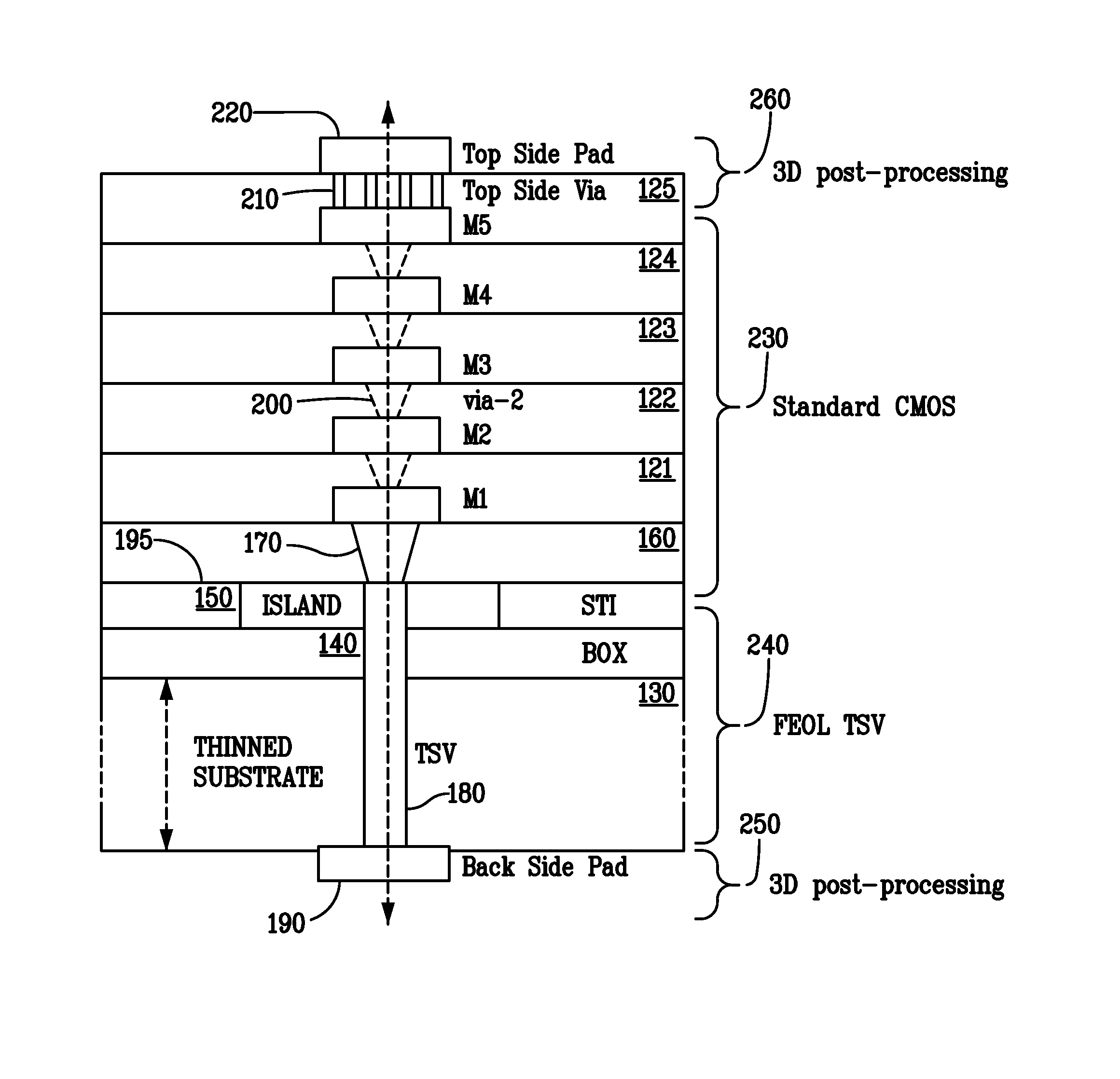
[0021]We will describe an exemplary embodiment that we have implemented in silicon using SOI (Silicon-on-Insulator) CMOS processes. The exemplary embodiment is a 3D-stackable 12 mm×12 mm structured ASIC die that has 42K interconnects and that is resource compatible with existing 2D structured ASIC devices of the same size. The exemplary 3D structured ASIC platform was designed and fabricated in our 0.35-μm foundry. It includes high-density front-end-of-line through silicon vias (TSVs) that we developed to implement the 3D vertical interconnects, as explained below.
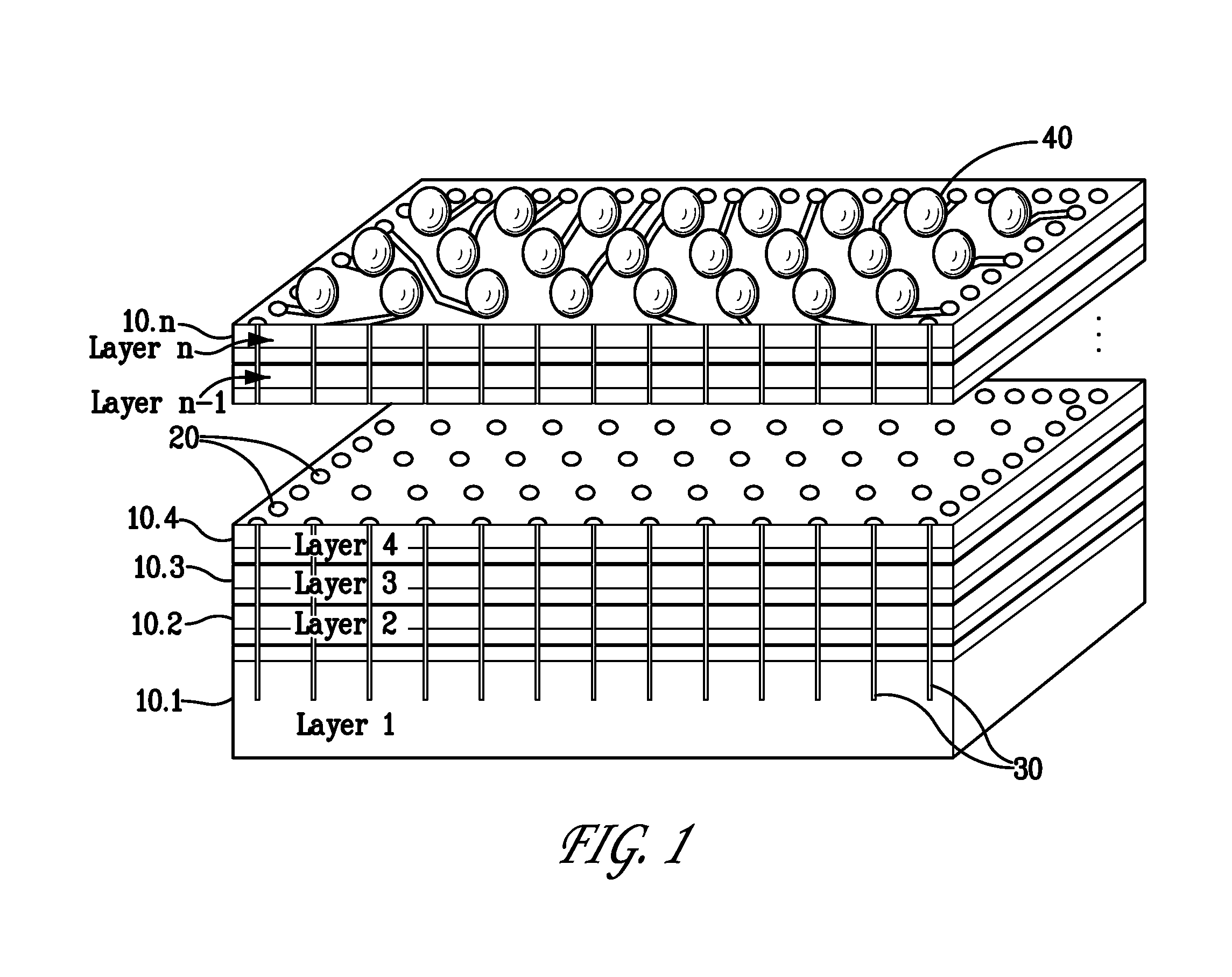
[0022]A simplified drawing of such a 3D vertical stack is provided in FIG. 1, where each of layers 10.1-10.n is a two-dimensional die connected to the neighbors above and below it by way of a fixed pattern of 3D interconnects 20. The three-dimensional interconnections are facilitated by an array of through-silicon vias (TSVs) 30. A ball-grid array 40, to which the input and output contacts have been redistributed, is shown...
PUM
 Abstract
Description
Claims
Application Information