
Semiconductor device and method for manufacturing the same

a semiconductor and semiconductor technology, applied in the field of oxide semiconductors, can solve the problems of unclear adverse effects of impurities on oxide semiconductors, and achieve the effect of reducing the concentration of nitrogen in oxide semiconductor layers

Active Publication Date: 2015-11-24
SEMICON ENERGY LAB CO LTD
View PDF155 Cites 6 Cited by
  • Summary
  • Abstract
  • Description
  • Claims
  • Application Information

AI Technical Summary

Benefits of technology

The patent describes a method to reduce the likelihood of hydrogen entering an oxide semiconductor layer. By decreasing the nitrogen concentration in this layer, hydrogen can be prevented from entering and forming a layer that is difficult for hydrogen to enter. This results in a more robust and reliable material for use in semiconductor devices.

Problems solved by technology

In particular, an adverse effect of an impurity on an oxide semiconductor has been still unclear.

Method used


Image

  • Semiconductor device and method for manufacturing the same
  • Semiconductor device and method for manufacturing the same
  • Semiconductor device and method for manufacturing the same

Examples


embodiment 1

[0049]An example of a method for manufacturing a semiconductor device will be described.

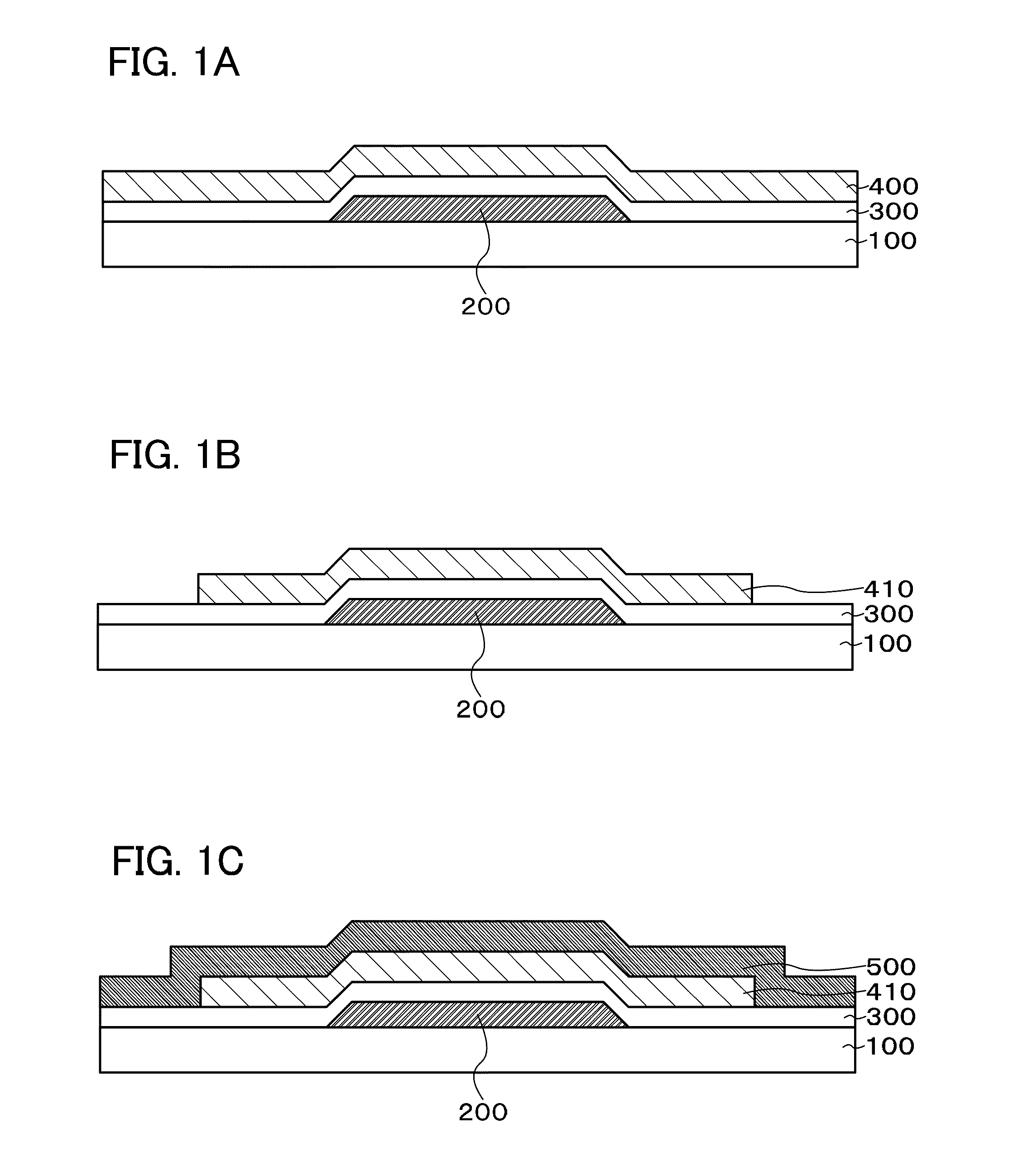
[0050]First, a gate electrode 200 is formed over a substrate 100 having an insulating surface. Then, a gate insulating layer 300 is formed over the gate electrode 200, and an oxide semiconductor layer 400 is formed over the gate insulating layer 300 (FIG. 1A).

[0051]As the substrate, any material can be used. For example, a glass substrate, a quartz substrate, a metal substrate, a plastic substrate, or a semiconductor substrate can be used, but the substrate is not limited to these examples.

[0052]In the case where an insulating substrate is used as the substrate, the substrate has an insulating surface.

[0053]On the other hand, in the case where a metal substrate, a semiconductor substrate, or the like is used as the substrate, the substrate can have an insulating surface when a base insulating layer is formed over the substrate.

[0054]Note that a base insulating layer may be formed over the substra...

embodiment 2

[0171]In this embodiment, a semiconductor device including a transistor which has a structure different from that of the transistor in Embodiment 1 will be described.

[0172]Note that materials or the like of the layers are the same as those in Embodiment 1.

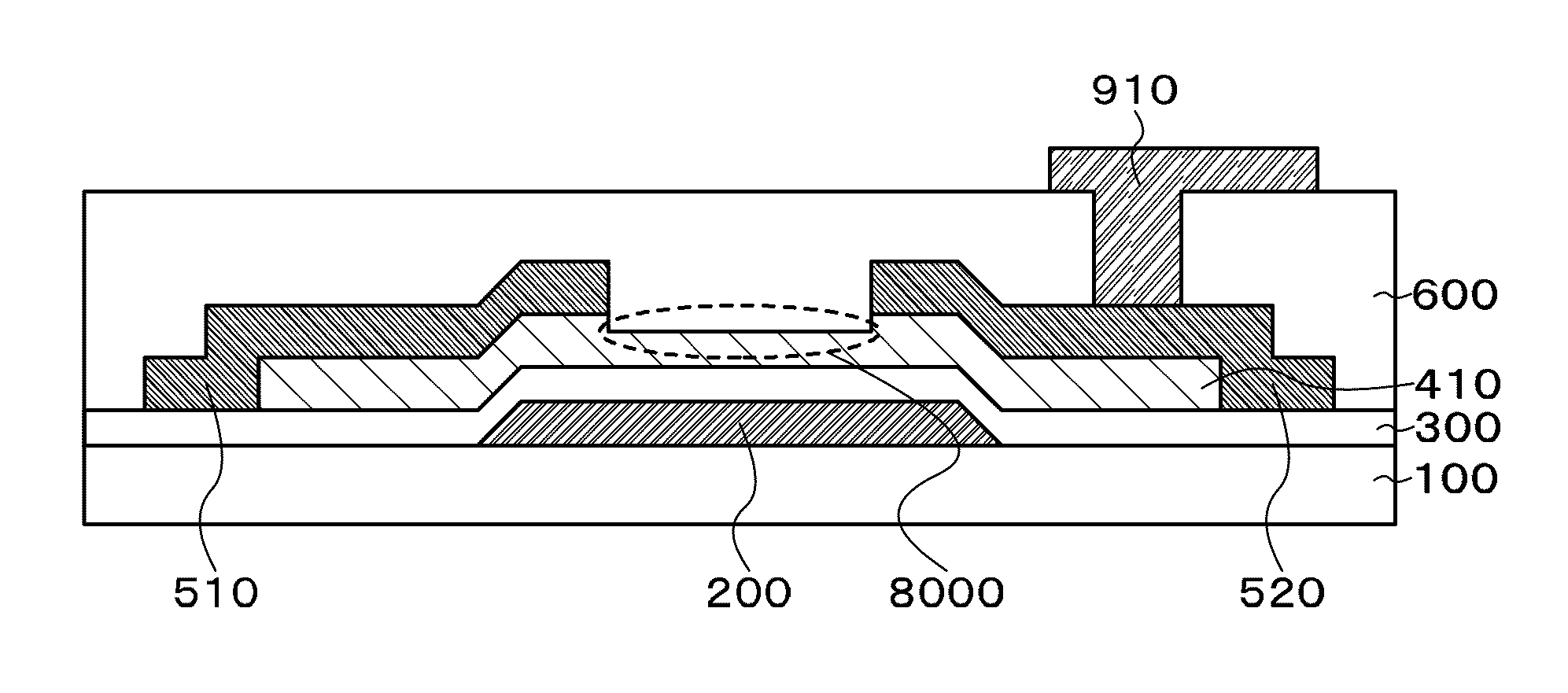
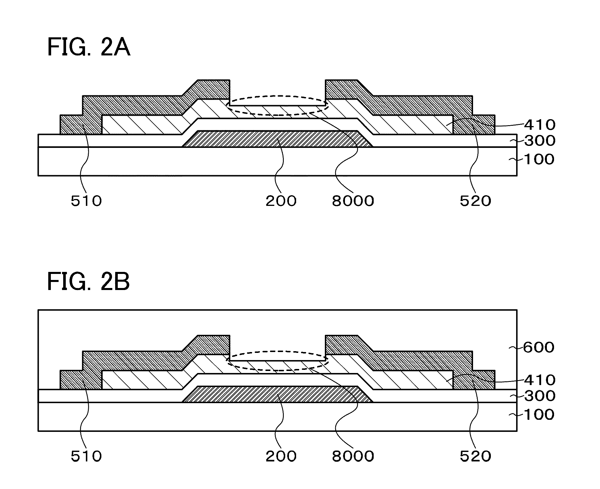
[0173]A transistor in FIG. 4A is a bottom-gate bottom-contact (BGBC) transistor, and includes the gate electrode 200 provided over the substrate 100 having an insulating surface; the gate insulating layer 300 provided over the gate electrode 200; the contact electrode 510 and the contact electrode 520 provided over the gate insulating layer 300; and the oxide semiconductor layer 410 (island shape) provided over the gate insulating layer 300, the contact electrode 510, and the contact electrode 520.

[0174]Note that the insulating layer 600 is provided to cover the transistor.

[0175]A portion surrounded by the dashed line 8000 serves as a back channel.

[0176]A transistor in FIG. 4B is a top-gate transistor, and includes the oxide semico...

embodiment 3

[0207]An example of a method for manufacturing the semiconductor device in FIG. 4A will be described.

[0208]Note that materials, conditions of heat treatment, and the like are the same as those in another embodiment.

[0209]The gate electrode 200 is formed over the substrate 100 having an insulating surface. Then, the gate insulating layer 300 is formed over the gate electrode 200, and the contact electrode 510 and the contact electrode 520 are formed over the gate insulating layer 300 (FIG. 5A).

[0210]Next, the oxide semiconductor layer 400 is formed over the gate insulating layer 300, the contact electrode 510, and the contact electrode 520 (FIG. 5B).

[0211]Next, the oxide semiconductor layer is subjected to first heat treatment.

[0212]The conditions of the first heat treatment are the same as those in Embodiment 1.

[0213]The first heat treatment may be performed after the oxide semiconductor layer 400 is etched into an island shape to form the oxide semiconductor layer 410.

[0214]However...


PUM


Abstract

Many of the physical properties of a silicon semiconductor have already been understood, whereas many of the physical properties of an oxide semiconductor have been still unclear. In particular, an adverse effect of an impurity on an oxide semiconductor has been still unclear. In view of the above, a structure is disclosed in which an impurity that influences electrical characteristics of a semiconductor device including an oxide semiconductor layer is prevented or is eliminated. A semiconductor device which includes a gate electrode, an oxide semiconductor layer, and a gate insulating layer provided between the gate electrode and the oxide semiconductor layer and in which the nitrogen concentration in the oxide semiconductor layer is 1×10²⁰ atoms / cm3 or less is provided.

Description

TECHNICAL FIELD[0001]The present invention relates to an oxide semiconductor.BACKGROUND ART[0002]A semiconductor device including an oxide semiconductor is disclosed in Patent Document 1.REFERENCEPatent Document[0003][Patent Document 1] Japanese Published Patent Application No. 2007-123861DISCLOSURE OF INVENTION[0004]Many of the physical properties of a silicon semiconductor have already been understood, whereas many of the physical properties of an oxide semiconductor have been still unclear.[0005]In particular, an adverse effect of an impurity on an oxide semiconductor has been still unclear.[0006]In view of the above, a structure will be disclosed in which an impurity that influences electrical characteristics of a semiconductor device including an oxide semiconductor layer is prevented or is eliminated.[0007]There are two factors of carriers in an oxide semiconductor layer.[0008]The first factor is oxygen deficiency in an oxide semiconductor layer.[0009]The second factor is a do...

Claims


Application Information

Patent Timeline
Patent Type & Authority Patents(United States)
IPC IPC(8): H01L21/336H01L29/786
CPCH01L29/7869H01L21/324H01L29/06H01L27/124H01L29/24
Inventor SAKATA, JUNICHIROMARUYAMA, TETSUNORIIMOTO, YUKI
Owner SEMICON ENERGY LAB CO LTD
Learn More