On-chip path-entangled photonic sources based on periodical poling and waveguide circuits in ferroelectric crystals

a ferroelectric crystal and path-entangled technology, applied in the field of quantum information technology, can solve the problems of large, fast and precise phase control of photons, and improve the efficiency of spd

Active Publication Date: 2016-03-01
NANJING UNIV
View PDF1 Cites 13 Cited by
  • Summary
  • Abstract
  • Description
  • Claims
  • Application Information

AI Technical Summary

Benefits of technology

[0008]The beneficial effects of this disclosure are based on several features of ferroelectric crystals. We take lithium niobate as the example. Firstly, the nonlinear coefficient is large and can be engineered artificially which enables the generation of bright photon pairs by fulfilling the quasi-phase-matching condition in the SPDC process. Moreover, the wavelength of entangled photons can be flexibly designed through changing the poling period. Secondly, the lithium niobate contains large electro-optic coefficient which can realize fast and precise phase control of photons. The repa...

Problems solved by technology

This photon pair from either path will interfere at the directional coupler, re...

Method used


Image

  • On-chip path-entangled photonic sources based on periodical poling and waveguide circuits in ferroelectric crystals
  • On-chip path-entangled photonic sources based on periodical poling and waveguide circuits in ferroelectric crystals
  • On-chip path-entangled photonic sources based on periodical poling and waveguide circuits in ferroelectric crystals

Examples


Embodiment Construction

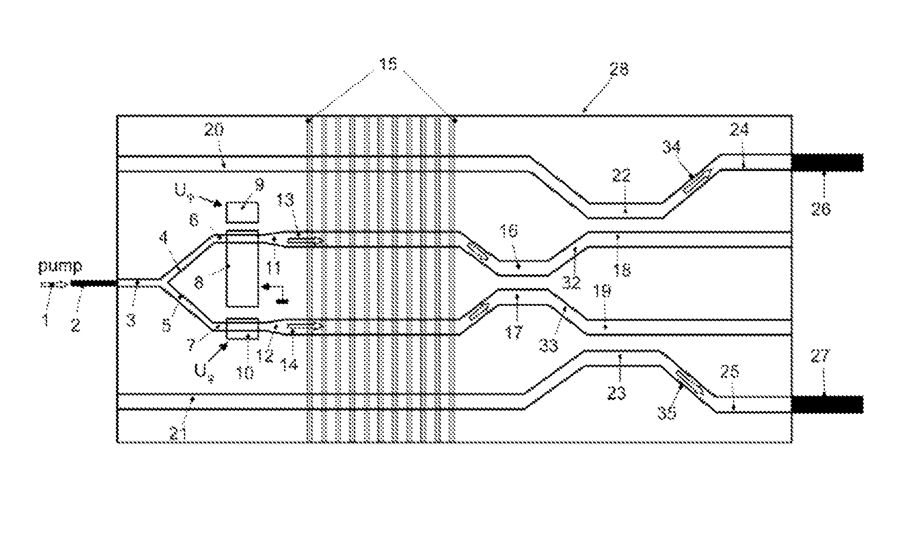
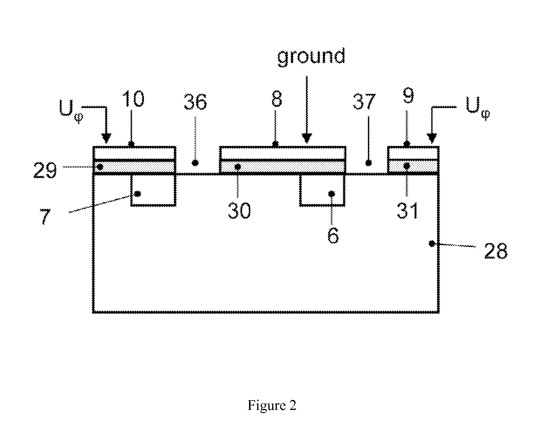
[0013]The following is the detailed instruction of LN photonic chip. On a single z-cut LN substrate, there are periodically poling structures for the generation of entangled photons, waveguide circuits for manipulating the pump laser and entangled photons and the eletrooptic modulator for controlling the phase of photons. The chip can be divided into three regions. Region I manipulates the classical pump laser, including the beam-splitting and EO phase-modulation. Region II is the periodical poling region wherein the nonlinear process takes place. It converts the pump beam into entangled photons through quasi-phase-matched SPDC process. The photon pair emits from either one of two paths, constructing a bunched state (|2,0>+eiφ|0,2>) / √{square root over (2)}. Region III manipulates the entangled photons, realizing Hong-Ou-Mandel (HOM) interference on the waveguide directional coupler. If two-photon phases from two paths are identical, the bunched state will convert into a deterministi...


PUM


Abstract

A photonic chip based on periodical poling and waveguides circuits in ferroelectric crystals, the method is based on the integration of waveguide circuits, periodical poling and electro-optic modulator (EOM). The chip is illustrated by FIG. 1. The waveguide circuits guide the photons and makes linear operations like the beam splitting, filtering etc. on the photons. The periodical poling enables the efficient spontaneous parametric down conversion (SPDC), resulting the generation of entangled photons. The EOM controls the phase of photons dynamically. The following directional coupler distributes the entangled photons and the quantum interference takes place, resulting different types of path-entangled states by controlling the voltage of EOM insides the chip.

Description

CROSS REFERENCE TO RELATED APPLICATION[0001]This application claims priority to Chinese Application No. 2014105511732, filed on Oct. 16, 2014. The Chinese Application is incorporated herein by reference in its entirety.FIELD OF THE INVENTION[0002]The present disclosure is generally directed at both quantum information technologies, photo-electronic technologies, nonlinear optic and more specifically it is directed at integrated quantum optics.BACKGROUND OF THE INVENTION[0003]Photonic entanglement is the key resource in quantum technologies such as quantum communication, quantum computing, therefore to engineer the entangled sources especially with controllability, high-efficiency, stability and portability has always been a popular topic in the quantum community. Traditionally the ways to generate entangled photons include: (1) the atomic transition [1]; (2) four-wave-mixing (FWM) in the atomic ensembles [2]; (3) FWM in silicon, silica-on-silicon [3,4] or fibers [5,6]; (4) Spontaneo...

Claims


Application Information

Patent Timeline
IPC IPC(8): G02B6/12
CPCG02B6/12033G02B6/12011G02B6/12014G02B6/12019G02B6/12016G02B2006/1204G02B2006/1215G02B2006/12159G02B2006/12142G02B2006/12152G02F1/3558G02F1/21G02F1/3775
Inventor XU, PINGJIN, HUAZHU, SHINING
Owner NANJING UNIV
Why Eureka
Try Eureka